The original schematic and files were designed and downloaded as Altium designer files. Afte they were edited to make the dev board, this repo was used: https://github.com/thesourcerer8/altium2kicad to convert the altium designer files from altium to KiCad. Then, these files still neded editing in KiCad, eventyally leading to the filal KiCad file. It is reccomended to use the Altium files if you intend to print of use the board, but if you insist on KiCad, just check for errors (unconnected pads) on the pcb, if you spot any fix ut, email me for the fix or open an issue and you will be good to go. I would be more than happy if anyone checked the KiCad files and aproved their functionality, or design the board from the beggining for KiCad. Its not very complex circuit, last time i checked the KiCad pcb was file, wihtout weird connections
Dc-Dc schematic From datasheet:

Edited Altium Designer PCB [dc-dc schematic] as a dev board, 3D view:

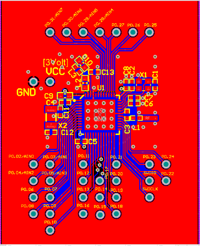
Edited Altium Designer PCB [dc-dc schematic] as a dev board, 2D view:
Edited KiCad PCB, 2D

Edited KiCad PCB, 3D

REFERENCE LAYOUT FOUND HERE [QFN48]: https://www.nordicsemi.com/?sc_itemid=%7B7CBDF55C-9745-4A7D-A491-5B66AE9454B6%7D
Questions? issues? email me: basilisvirus@hotmail.com