English | 中文
This guide is written for developers who wish to start programming microcontrollers using GCC compiler and a datasheet - nothing else! The fundamentals explained in this guide, will help you understand better how frameworks like Cube, Keil, Arduino - and others, work.
The guide covers the following topics: memory and registers, interrupt vector
table, startup code, linker script, build automation using make, GPIO
peripheral and LED blinky, SysTick timer, UART peripheral and debug output,
printf redirect to UART (IO retargeting), debugging with Segger Ozone,
system clock setup, web server implementation with device dashboard, and
automatic tests (including
automatic tests on a real hardware).
Every chapter in this guide comes with a complete source code which gradually progress in functionality and completeness. The last (web server) chapter is the most complete, and can be used as a skeleton for the project of your own, dear reader. Therefore, that last example project is provided for the other boards too. This tutorial uses the Nucleo-F429ZI development board, so go ahead and download the "mcu datasheet" and the "board datasheet" for it.
| Board | MCU datasheet | Board datasheet | Status | Skeleton project |
|---|---|---|---|---|
| STM32 Nucleo-F429ZI | mcu datasheet | board datasheet | complete | link |
| TI EK-TM4C1294XL | mcu datasheet | board datasheet | complete | link |
| RP2040 Pico-W5500 | mcu datasheet | board datasheet | complete | link |
Feel free to file an issue to support the board you work with.
To proceed, the following tools are required:
- ARM GCC, https://launchpad.net/gcc-arm-embedded - for compiling and linking
- GNU make, http://www.gnu.org/software/make/ - for build automation
- ST link, https://github.com/stlink-org/stlink - for flashing
Start a terminal, and execute:
$ /bin/bash -c "$(curl -fsSL https://raw.githubusercontent.com/Homebrew/install/HEAD/install.sh)"
$ brew install gcc-arm-embedded make stlinkStart a terminal, and execute:
$ sudo apt -y update
$ sudo apt -y install gcc-arm-none-eabi make stlink-tools- Download and install gcc-arm-none-eabi-10.3-2021.10-win32.exe. Enable "Add path to environment variable" during the installation
- Create
c:\toolsfolder - Download stlink-1.7.0-x86_64-w64-mingw32.zip and unpack
bin/st-flash.exeintoc:\tools - Download make-4.4-without-guile-w32-bin.zip and unpack
bin/make.exeintoc:\tools - Add
c:\toolsto thePathenvironment variable - Verify installation:
- Download and unzip this repository into
c:\ - Start command prompt, and execute the following:
C:\Users\YOURNAME> cd \
C:\> cd bare-metal-programming-guide-main\step-0-minimal
C:\bare-metal-programming-guide-main\step-0-minimal> make
arm-none-eabi-gcc main.c  -W -Wall -Wextra -Werror ...
- Download and unzip this repository into
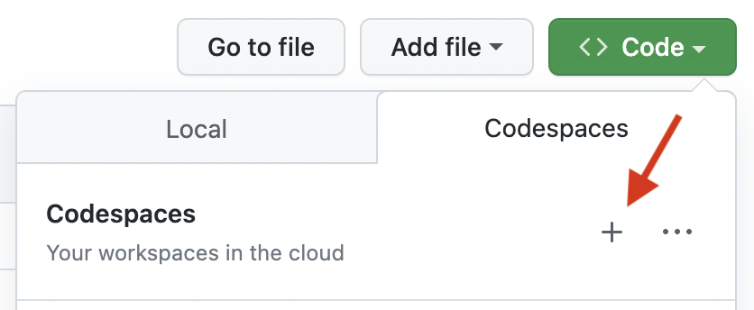
- Click on the "Code" button, select "Codespaces" tab, click on plus icon
- This repository will be opened in the in-browser editor, with an opened terminal:

- Execute Linux/Ubuntu setup instructions in the terminal:
sudo apt -y update
sudo apt -y install gcc-arm-none-eabi make stlink-tools
- Verify that the build process works:
cd step-4-printf
make firmware.bin
A microcontroller (uC, or MCU) is a small computer. Typically it has CPU, RAM, flash to store firmware code, and a bunch of pins that stick out. Some pins are used to power the MCU, usually marked as GND (ground) and VCC pins. Other pins are used to communicate with the MCU, by means of high/low voltage applied to those pins. One of the simplest ways of communication is an LED attached to a pin: one LED contact is attached to the ground pin (GND), and another contact is attached to a signal pin via a current-limiting resistor. A firmware code can set high or low voltage on a signal pin, making LED blink:
The 32-bit address space of the MCU is divided by regions. For example, some region of memory is mapped to the internal MCU flash at a specific address. Firmware code instructions are read and executed by reading from that memory region. Another region is RAM, which is also mapped to a specific address. We can read and write any values to the RAM region.
From STM32F429 datasheet, we can take a look at section 2.3.1 and learn that RAM region starts at address 0x20000000 and has size of 192KB. From section 2.4 we can learn that flash is mapped at address 0x08000000. Our MCU has 2MB flash, so flash and RAM regions are located like this:
From the datasheet we can also learn that there are many more memory regions. Their address ranges are given in the section 2.3 "Memory Map". For example, there is a "GPIOA" region that starts at 0x40020000 and has length of 1KB.
These memory regions correspond to a different "peripherals" inside the MCU - a piece of silicon circuitry that make certain pins behave in a special way. A peripheral memory region is a collection of 32-bit registers. Each register is a 4-byte memory range at a certain address, that maps to a certain function of the given peripheral. By writing values into a register - in other words, by writing a 32-bit value at a certain memory address, we can control how given peripheral should behave. By reading registers, we can read back peripheral's data or configuration.
There are many different peripherals. One of the simpler ones are GPIO (General Purpose Input Output), which allow user to set MCU pins into "output mode" and set high or low voltage on them. Or, set pins into an "input mode" and read voltage values from them. There is a UART peripheral which can transmit and receive serial data over two pins using serial protocol. There are many other peripherals.
Often, there are multiple "instances" of the same peripheral, for example GPIOA, GPIOB, ... which control different set of MCU pins. Likewise, there could be UART1, UART2, ... which allow to implement multiple UART channels. On Nucleo-F429, there are several GPIO and UART peripherals.
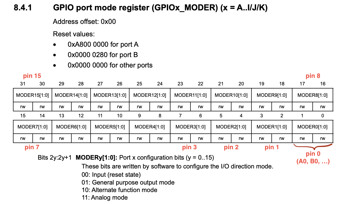
For example, GPIOA
peripheral starts at 0x40020000, and we can find GPIO register description in
section 8.4. The datasheet says that GPIOA_MODER register has offset 0, that
means that it's address is 0x40020000 + 0, and this is the format of the
register:
The datasheet shows that the 32-bit MODER register is a collection of 2-bit values, 16 in total. Therefore, one MODER register controls 16 physical pins, Bits 0-1 control pin 0, bits 2-3 control pin 1, and so on. The 2-bit value encodes pin mode: 0 means input, 1 means output, 2 means "alternate function" - some specific behavior described elsewhere, and 3 means analog. Since the peripheral name is "GPIOA", then pins are named "A0", "A1", etc. For peripheral "GPIOB", pin naming would be "B0", "B1", ...
If we write 32-bit value 0 to the register MODER, we'll set all 16 pins,
from A0 to A15, to input mode:
* (volatile uint32_t *) (0x40020000 + 0) = 0; // Set A0-A15 to input modeNote the volatile specifier. Its meaning will be covered later. By setting
individual bits, we can selectively set specific pins to a desired mode. For
example, this snippet sets pin A3 to output mode:
  * (volatile uint32_t *) (0x40020000 + 0) &= ~(3 << 6);  // CLear bit range 6-7
  * (volatile uint32_t *) (0x40020000 + 0) |= 1 << 6;     // Set bit range 6-7 to 1
Let me explain those bit operations. Our goal is to set bits 6-7, which are responsible for the pin 3 of GPIOA peripheral, to a specific value (1, in our case). This is done in two steps. First, we must clear the current value of bits 6-7, because it may hold some value already. Then we must set bits 6-7 to the value we want.
So, first, we must set bit range 6-7 (two bits at position 6) to zero. How do we set a number of bits to zero? In four steps:
| Action | Expression | Bits (first 12 of 32) |
|---|---|---|
Get a number with N contiguous bits set: 2^N-1, N=2 |
3 |
000000000011 |
| Shift that number X positions left | (3<<6) |
000011000000 |
| Invert the number: turn zeros to ones, and ones to zeroes | ~(3<<6) |
111100111111 |
| Logical AND with existing value | VAL &= ~(3<<6) |
xxxx00xxxxxx |
Note that the last operation, logical AND, turns N bits at position X to zero (because they are ANDed with 0), but retains the value of all other bits (because they are ANDed with 1). Retaining existing value is important, cause we don't want to change settings in other bit ranges. So in general, if we want to clear N bits at position X:
REGISTER &= ~((2^N - 1) << X);And, finally, we want to set a given bit range to the value we want. We shift that value X positions left, and OR with the current value of the whole register (in order to retain other bits' values):
REGISTER |= VALUE << X;In the previous section we have learned that we can read and write peripheral register by direct accessing certain memory addresses. Let's look at the snippet that sets pin A3 to output mode:
  * (volatile uint32_t *) (0x40020000 + 0) &= ~(3 << 6);  // CLear bit range 6-7
  * (volatile uint32_t *) (0x40020000 + 0) |= 1 << 6;     // Set bit range 6-7 to 1
That is pretty cryptic. Without extensive comments, such code would be quite hard to understand. We can rewrite this code to a much more readable form. The idea is to represent the whole peripheral as a structure that contains 32-bit fields. Let's see what registers exist for the GPIO peripheral in the section 8.4 of the datasheet. They are MODER, OTYPER, OSPEEDR, PUPDR, IDR, ODR, BSRR, LCKR, AFR. Their offsets are with offsets 0, 4, 8, etc... . That means we can represent them as a structure with 32-bit fields, and make a define for GPIOA:
struct gpio {
  volatile uint32_t MODER, OTYPER, OSPEEDR, PUPDR, IDR, ODR, BSRR, LCKR, AFR[2];
};

#define GPIOA ((struct gpio *) 0x40020000)
Then, for setting GPIO pin mode, we can define a function:
// Enum values are per datasheet: 0, 1, 2, 3
enum {GPIO_MODE_INPUT, GPIO_MODE_OUTPUT, GPIO_MODE_AF, GPIO_MODE_ANALOG};

static inline void gpio_set_mode(struct gpio *gpio, uint8_t pin, uint8_t mode) {
  gpio->MODER &= ~(3U << (pin * 2));        // Clear existing setting
  gpio->MODER |= (mode & 3) << (pin * 2);   // Set new mode
}
Now, we can rewrite the snippet for A3 like this:
gpio_set_mode(GPIOA, 3 /* pin */, GPIO_MODE_OUTPUT); // Set A3 to outputOur MCU has several GPIO peripherals (also called "banks"): A, B, C, ... K. From section 2.3 we can see that they are 1KB away from each other: GPIOA is at address 0x40020000, GPIOB is at 0x40020400, and so on:
#define GPIO(bank) ((struct gpio *) (0x40020000 + 0x400 * (bank)))We can create pin numbering that includes the bank and the pin number.
To do that, we use 2-byte uint16_t value, where upper byte indicates
GPIO bank, and lower byte indicates pin number:
#define PIN(bank, num) ((((bank) - 'A') << 8) | (num))
#define PINNO(pin) (pin & 255)
#define PINBANK(pin) (pin >> 8)
This way, we can specify pins for any GPIO bank:
  uint16_t pin1 = PIN('A', 3);    // A3   - GPIOA pin 3
  uint16_t pin2 = PIN('G', 11);   // G11  - GPIOG pin 11
Let's rewrite the gpio_set_mode() function to take our pin specification:
static inline void gpio_set_mode(uint16_t pin, uint8_t mode) {
  struct gpio *gpio = GPIO(PINBANK(pin)); // GPIO bank
  uint8_t n = PINNO(pin);                 // Pin number
  gpio->MODER &= ~(3U << (n * 2));        // Clear existing setting
  gpio->MODER |= (mode & 3) << (n * 2);   // Set new mode
}
Now the code for A3 is self-explanatory:
  uint16_t pin = PIN('A', 3);            // Pin A3
  gpio_set_mode(pin, GPIO_MODE_OUTPUT);  // Set to output
Note that we have created a useful initial API for the GPIO peripheral. Other peripherals, like UART (serial communication) and others - can be implemented in a similar way. This is a good programming practice that makes code self-explanatory and human readable.
When an ARM MCU boots, it reads a so-called "vector table" from the beginning of flash memory. A vector table is a concept common to all ARM MCUs. That is a array of 32-bit addresses of interrupt handlers. First 16 entries are reserved by ARM and are common to all ARM MCUs. The rest of interrupt handlers are specific to the given MCU - these are interrupt handlers for peripherals. Simpler MCUs with few peripherals have few interrupt handlers, and more complex MCUs have many.
Vector table for STM32F429 is documented in Table 62. From there we can learn that there are 91 peripheral handlers, in addition to the standard 16.
Every entry in the vector table is an address of a function that MCU executes when a hardware interrupt (IRQ) triggers. The exception are first two entries, which play a key role in the MCU boot process. Those two first values are: an initial stack pointer, and an address of the boot function to execute (a firmware entry point).
So now we know, that we must make sure that our firmware should be composed in a way that the 2nd 32-bit value in the flash should contain an address of out boot function. When MCU boots, it'll read that address from flash, and jump to our boot function.
Let's create a file main.c, and specify our boot function that initially does
nothing (falls into infinite loop), and specify a vector table that contains 16
standard entries and 91 STM32 entries. In your editor of choice, create
main.c file and copy/paste the following into main.c file:
// Startup code
__attribute__((naked, noreturn)) void _reset(void) {
  for (;;) (void) 0;  // Infinite loop
}

extern void _estack(void);  // Defined in link.ld

// 16 standard and 91 STM32-specific handlers
__attribute__((section(".vectors"))) void (*tab[16 + 91])(void) = {
  _estack, _reset
};
For function _reset(), we have used GCC-specific attributes naked and
noreturn - they mean, standard function's prologue and epilogue should not
be created by the compiler, and that function does not return.
The void (*tab[16 + 91])(void) expression means: define an array of 16 + 91
pointers to functions, that return nothing (void) and take to arguments. Each
such function is an IRQ handler (Interrupt ReQuest handler). An array of those
handlers is called a vector table.
The vector table tab we put in a separate section called .vectors - that we
need later to tell the linker to put that section right at the beginning of the
generated firmware - and consecutively, at the beginning of flash memory. The
first two entries are: the value of the stack pointer register, and the
firmware's entry point. We leave the rest of vector table filled with zeroes.
Let's compile our code. Start a terminal (or a command prompt on Windows) and execute:
$ arm-none-eabi-gcc -mcpu=cortex-m4 main.c -cThat works! The compilation produced a file main.o which contains
our minimal firmware that does nothing. The main.o file is in ELF binary
format, which contains several sections. Let's see them:
$ arm-none-eabi-objdump -h main.o
...
Idx Name          Size      VMA       LMA       File off  Algn
  0 .text         00000002  00000000  00000000  00000034  2**1
                  CONTENTS, ALLOC, LOAD, READONLY, CODE
  1 .data         00000000  00000000  00000000  00000036  2**0
                  CONTENTS, ALLOC, LOAD, DATA
  2 .bss          00000000  00000000  00000000  00000036  2**0
                  ALLOC
  3 .vectors      000001ac  00000000  00000000  00000038  2**2
                  CONTENTS, ALLOC, LOAD, RELOC, DATA
...
Note that VMA/LMA addresses for sections are set to 0 - meaning, main.o
is not yet a complete firmware, because it does not contain the information
where those section should be loaded in the address space. We need to use
a linker to produce a full firmware firmware.elf from main.o.
The section .text contains firmware code, in our case it is just a _reset()
function, 2-bytes long - a jump instruction to its own address. There is
an empty .data section and an empty .bss section
(data that is initialized to zero) . Our firmware will be copied
to the flash region at offset 0x8000000, but our data section should reside
in RAM - therefore our _reset() function should copy the contents of the
.data section to RAM. Also it has to write zeroes to the whole .bss
section. Our .data and .bss sections are empty, but let's modify our
_reset() function anyway to handle them properly.
In order to do all that, we must know where stack starts, and where data and bss section start. This we can specify in the "linker script", which is a file with the instructions to the linker, where to put various sections in the address space, and which symbols to create.
Create a file link.ld, and copy-paste contents from
step-0-minimal/link.ld. Below is the explanation:
ENTRY(_reset);
This line tells the linker the value of the "entry point" attribute in the generated ELF header - so this is a duplicate to what a vector table has. This is an aid for a debugger (like Ozone, described below) that helps to set a breakpoint at the beginning of the firmware. A debugger does not know about a vector table, so it relies on the ELF header.
MEMORY {
  flash(rx)  : ORIGIN = 0x08000000, LENGTH = 2048k
  sram(rwx) : ORIGIN = 0x20000000, LENGTH = 192k  /* remaining 64k in a separate address space */
}
This tells the linker that we have two memory regions in the address space, their addresses and sizes.
_estack = ORIGIN(sram) + LENGTH(sram); /* stack points to end of SRAM */
This tell a linker to create a symbol estack with value at the very end
of the RAM memory region. That will be our initial stack value!
  .vectors  : { KEEP(*(.vectors)) }   > flash
  .text     : { *(.text*) }           > flash
  .rodata   : { *(.rodata*) }         > flash
These lines tell the linker to put vectors table on flash first,
followed by .text section (firmware code), followed by the read only
data .rodata.
The next goes .data section:
  .data : {
    _sdata = .;   /* .data section start */
    *(.first_data)
    *(.data SORT(.data.*))
    _edata = .;  /* .data section end */
  } > sram AT > flash
  _sidata = LOADADDR(.data);
Note that we tell linker to create _sdata and _edata symbols. We'll
use them to copy data section to RAM in the _reset() function.
Same for .bss section:
  .bss : {
    _sbss = .;              /* .bss section start */
    *(.bss SORT(.bss.*) COMMON)
    _ebss = .;              /* .bss section end */
  } > sram
Now we can update our _reset() function. We copy .data section to RAM, and
initialise bss section to zeroes. Then, we call main() function - and fall into
infinite loop in case if main() returns:
int main(void) {
  return 0; // Do nothing so far
}

// Startup code
__attribute__((naked, noreturn)) void _reset(void) {
  // memset .bss to zero, and copy .data section to RAM region
  extern long _sbss, _ebss, _sdata, _edata, _sidata;
  for (long *src = &_sbss; src < &_ebss; src++) *src = 0;
  for (long *src = &_sdata, *dst = &_sidata; src < &_edata;) *src++ = *dst++;

  main();             // Call main()
  for (;;) (void) 0;  // Infinite loop in the case if main() returns
}
The following diagram visualises how _reset() initialises .data and .bss:
The firmware.bin file is just a concatenation of the three sections:
.vectors (IRQ vector table), .text (code) and .data (data). Those
sections were built according to the linker script: .vectors lies at the very
beginning of flash, then .text follows immediately after, and .data lies
far above. Addresses in .text are in the flash region, and addresses in
.data are in the RAM region. If some function has address e.g. 0x8000100,
then it it located exactly at that address on flash. But if the code accesses
some variable in the .data section by the address e.g. 0x20000200, then
there is nothing at that address, because at boot, .data section in the
firmware.bin resides in flash! That's why the startup code must relocate
.data section from flash region to the RAM region.
Now we are ready to produce a full firmware file firmware.elf:
$ arm-none-eabi-gcc -T link.ld -nostdlib main.o -o firmware.elfLet's examine sections in firmware.elf:
$ arm-none-eabi-objdump -h firmware.elf
...
Idx Name          Size      VMA       LMA       File off  Algn
  0 .vectors      000001ac  08000000  08000000  00010000  2**2
                  CONTENTS, ALLOC, LOAD, DATA
  1 .text         00000058  080001ac  080001ac  000101ac  2**2
                  CONTENTS, ALLOC, LOAD, READONLY, CODE
...
Now we can see that the .vectors section will reside at the very beginning of flash memory at address 0x8000000, then the .text section right after it, at 0x80001ac. Our code does not create any variables, so there is no data section.
We're ready to flash this firmware! First, extract sections from the firmware.elf into a single contiguous binary blob:
$ arm-none-eabi-objcopy -O binary firmware.elf firmware.binAnd use st-link utility to flash the firmware.bin. Plug your board to the
USB, and execute:
$ st-flash --reset write firmware.bin 0x8000000Done! We've flashed a firmware that does nothing.
Instead of typing those compilation, linking and flashing commands, we can
use make command line tool to automate the whole process. make utility
uses a configuration file named Makefile where it reads instructions
how to execute actions. This automation is great because it also documents the
process of building firmware, used compilation flags, etc.
There is a great Makefile tutorial at https://makefiletutorial.com - for those
new to make, I suggest to take a look. Below, I list the most essential
concepts required to understand our simple bare metal Makefile. Those who
already familiar with make, can skip this section.
The Makefile format is simple:
action1:
	command ...     # Comments can go after hash symbol
	command ....    # IMPORTANT: command must be preceded with the TAB character

action2:
	command ...     # Don't forget about TAB. Spaces won't work!
Now, we can invoke make with the action name (also called target) to execute
a corresponding action:
$ make action1It is possible to define variables and use them in commands. Also, actions can be file names that needs to be created:
firmware.elf:
	COMPILATION COMMAND .....
And, any action can have a list of dependencies. For example, firmware.elf
depends on our source file main.c. Whenever main.c file changes, the
make build command rebuilds firmware.elf:
build: firmware.elf

firmware.elf: main.c
	COMPILATION COMMAND
Now we are ready to write a Makefile for our firmware. We define a build
action / target:
CFLAGS  ?=  -W -Wall -Wextra -Werror -Wundef -Wshadow -Wdouble-promotion \
            -Wformat-truncation -fno-common -Wconversion \
            -g3 -Os -ffunction-sections -fdata-sections -I. \
            -mcpu=cortex-m4 -mthumb -mfloat-abi=hard -mfpu=fpv4-sp-d16 $(EXTRA_CFLAGS)
LDFLAGS ?= -Tlink.ld -nostartfiles -nostdlib --specs nano.specs -lc -lgcc -Wl,--gc-sections -Wl,-Map=$@.map
SOURCES = main.c

build: firmware.elf

firmware.elf: $(SOURCES)
	arm-none-eabi-gcc $(SOURCES) $(CFLAGS) $(LDFLAGS) -o $@
There, we define compilation flags. The ?= means that's a default value;
we could override them from the command line like this:
$ make build CFLAGS="-O2 ...."We specify CFLAGS, LDFLAGS and SOURCES variables.
Then we tell make: if you're told to build, then create a firmware.elf
file. It depends on the main.c file, and to create it, start
arm-none-eabi-gcc compiler with a given flags. $@ special variable
expands to a target name - in our case, firmware.elf.
Let's call make:
$ make build
arm-none-eabi-gcc main.c  -W -Wall -Wextra -Werror -Wundef -Wshadow -Wdouble-promotion -Wformat-truncation -fno-common -Wconversion -g3 -Os -ffunction-sections -fdata-sections -I. -mcpu=cortex-m4 -mthumb -mfloat-abi=hard -mfpu=fpv4-sp-d16  -Tlink.ld -nostartfiles -nostdlib --specs nano.specs -lc -lgcc -Wl,--gc-sections -Wl,-Map=firmware.elf.map -o firmware.elf
If we run it again:
$ make build
make: Nothing to be done for `build'.
The make utility examines modification times for main.c dependency and
firmware.elf - and does not do anything if firmware.elf is up to date.
But if we change main.c, then next make build will recompile:
$ touch main.c # Simulate changes in main.c
$ make build
Now, what is left - is the flash target:
firmware.bin: firmware.elf
	$(DOCKER) $(CROSS)-objcopy -O binary $< $@

flash: firmware.bin
	st-flash --reset write $(TARGET).bin 0x8000000
That's it! Now, make flash terminal command creates a firmware.bin file,
and flashes it to the board. It'll recompile the firmware if main.c changes,
because firmware.bin depends on firmware.elf, and it in turn depends on
main.c. So, now the development cycle would be these two actions in a loop:
# Develop code in main.c
$ make flash
It is a good idea to add a clean target to remove build artifacts:
clean:
	rm -rf firmware.*
A complete project source code you can find in step-0-minimal folder.
Now as we have the whole build / flash infrastructure set up, it is time to teach our firmware to do something useful. Something useful is of course blinking an LED. A Nucleo-F429ZI board has three built-in LEDs. In a Nucleo board datasheet section 6.5 we can see which pins built-in LEDs are attached to:
- PB0: green LED
- PB7: blue LED
- PB14: red LED
Let's modify main.c file and add our definitions for PIN, gpio_set_mode().
In the main() function, we set the blue LED to output mode, and start an
infinite loop. First, let's copy the definitions for pins and GPIO we have
discussed earlier. Note we also add a convenience macro BIT(position):
#include <inttypes.h>
#include <stdbool.h>

#define BIT(x) (1UL << (x))
#define PIN(bank, num) ((((bank) - 'A') << 8) | (num))
#define PINNO(pin) (pin & 255)
#define PINBANK(pin) (pin >> 8)

struct gpio {
  volatile uint32_t MODER, OTYPER, OSPEEDR, PUPDR, IDR, ODR, BSRR, LCKR, AFR[2];
};
#define GPIO(bank) ((struct gpio *) (0x40020000 + 0x400 * (bank)))

// Enum values are per datasheet: 0, 1, 2, 3
enum { GPIO_MODE_INPUT, GPIO_MODE_OUTPUT, GPIO_MODE_AF, GPIO_MODE_ANALOG };

static inline void gpio_set_mode(uint16_t pin, uint8_t mode) {
  struct gpio *gpio = GPIO(PINBANK(pin));  // GPIO bank
  int n = PINNO(pin);                      // Pin number
  gpio->MODER &= ~(3U << (n * 2));         // Clear existing setting
  gpio->MODER |= (mode & 3) << (n * 2);    // Set new mode
}
Some microcontrollers, when they are powered, have all their peripherals powered and enabled, automatically. STM32 MCUs, however, by default have their peripherals disabled in order to save power. In order to enable a GPIO peripheral, it should be enabled (clocked) via the RCC (Reset and Clock Control) unit. In the datasheet section 7.3.10 we find that the AHB1ENR (AHB1 peripheral clock enable register) is responsible to turn GPIO banks on or off. First we add a definition for the whole RCC unit:
struct rcc {
  volatile uint32_t CR, PLLCFGR, CFGR, CIR, AHB1RSTR, AHB2RSTR, AHB3RSTR,
      RESERVED0, APB1RSTR, APB2RSTR, RESERVED1[2], AHB1ENR, AHB2ENR, AHB3ENR,
      RESERVED2, APB1ENR, APB2ENR, RESERVED3[2], AHB1LPENR, AHB2LPENR,
      AHB3LPENR, RESERVED4, APB1LPENR, APB2LPENR, RESERVED5[2], BDCR, CSR,
      RESERVED6[2], SSCGR, PLLI2SCFGR;
};
#define RCC ((struct rcc *) 0x40023800)
In the AHB1ENR register documentation we see that bits from 0 to 8 inclusive set the clock for GPIO banks GPIOA - GPIOE:
int main(void) {
  uint16_t led = PIN('B', 7);            // Blue LED
  RCC->AHB1ENR |= BIT(PINBANK(led));     // Enable GPIO clock for LED
  gpio_set_mode(led, GPIO_MODE_OUTPUT);  // Set blue LED to output mode
  for (;;) (void) 0;                     // Infinite loop
  return 0;
}
Now, what is left to do, is to find out how to set a GPIO pin on and off, and then modify the main loop to set an LED pin on, delay, off, delay. Looking at the datasheet section 8.4.7, wee see that the register BSRR is responsible for setting voltage high or low. The low 16 bit are used to set the ODR register (i.e. set pin high), and high 16 bit are used to reset the ODR register (i.e. set pin low). Let's define an API function for that:
static inline void gpio_write(uint16_t pin, bool val) {
  struct gpio *gpio = GPIO(PINBANK(pin));
  gpio->BSRR = (1U << PINNO(pin)) << (val ? 0 : 16);
}
Next we need to implement a delay function. We do not require an accurate
delay at this moment, so let's define a function spin() that just executes
a NOP instruction a given number of times:
static inline void spin(volatile uint32_t count) {
  while (count--) (void) 0;
}
Finally, we're ready to modify our main loop to implement LED blinking:
  for (;;) {
    gpio_write(pin, true);
    spin(999999);
    gpio_write(pin, false);
    spin(999999);
  }
Run make flash and enjoy blue LED flashing.
A complete project source code you can find in step-1-blinky.
In order to implement an accurate time keeping, we should enable ARM's SysTick interrupt. SysTick a 24-bit hardware counter, and is part of ARM core, therefore it is documented by the ARM datasheet. Looking at the datasheet, we see that SysTick has four registers:
- CTRL - used to enable/disable systick
- LOAD - an initial counter value
- VAL - a current counter value, decremented on each clock cycle
- CALIB - calibration register
Every time VAL drops to zero, a SysTick interrupt is generated. The SysTick interrupt index in the vector table is 15, so we need to set it. Upon boot, our board Nucleo-F429ZI runs at 16Mhz. We can configure the SysTick counter to trigger interrupt each millisecond.
First, let's define a SysTick peripheral. We know 4 registers, and from the datasheet we can learn that the SysTick address is 0xe000e010. So:
struct systick {
  volatile uint32_t CTRL, LOAD, VAL, CALIB;
};
#define SYSTICK ((struct systick *) 0xe000e010)
Next, add an API function that configures it. We need to enable SysTick
in the SYSTICK->CTRL register, and also we must clock it via the
RCC->APB2ENR, described in the section 7.4.14:
#define BIT(x) (1UL << (x))
static inline void systick_init(uint32_t ticks) {
  if ((ticks - 1) > 0xffffff) return;  // Systick timer is 24 bit
  SYSTICK->LOAD = ticks - 1;
  SYSTICK->VAL = 0;
  SYSTICK->CTRL = BIT(0) | BIT(1) | BIT(2);  // Enable systick
  RCC->APB2ENR |= BIT(14);                   // Enable SYSCFG
}
By default, Nucleo-F429ZI board runs at 16Mhz. That means, if we call
systick_init(16000000 / 1000);, then SysTick interrupt will be generated
every millisecond. We should have interrupt handler function defined - here
it is, we simply increment a 32-bit millisecond counter:
static volatile uint32_t s_ticks; // volatile is important!!
void SysTick_Handler(void) {
  s_ticks++;
}
With 16MHz clock, we init SysTick counter to trigger an interrupt every
16000 cycles: the SYSTICK->VAL initial value is 15999, then it decrements
on each cycle by 1, and when it reaches 0, an interrupt is generated. The
firmware code execution gets interrupted: a SysTick_Handler() function is
called to increment s_tick variable. Here how it looks like on a time scale:
The volatile specifier is required here becase s_ticks is modified by the
interrupt handler. volatile prevents the compiler to optimise/cache s_ticks
value in a CPU register: instead, generated code always accesses memory. That
is why volatile keywords is present in the peripheral struct definitions,
too. Since this is important to understand, let's demonstrate that on a simple
function: Arduino's delay(). Let is use our s_ticks variable:
void delay(unsigned ms) {            // This function waits "ms" milliseconds
 uint32_t until = s_ticks + ms;      // Time in a future when we need to stop
 while (s_ticks < until) (void) 0;   // Loop until then
}
Now let's compile this code with, and without volatile specifier for s_ticks
and compare generated machine code:
// NO VOLATILE: uint32_t s_ticks;       |  // VOLATILE: volatile uint32_t s_ticks;
                                        |
 ldr     r3, [pc, #8]  // cache s_ticks |  ldr     r2, [pc, #12]
 ldr     r3, [r3, #0]  // in r3         |  ldr     r3, [r2, #0]   // r3 = s_ticks
 adds    r0, r3, r0    // r0 = r3 + ms  |  adds    r3, r3, r0     // r3 = r3 + ms
                                        |  ldr     r1, [r2, #0]   // RELOAD: r1 = s_ticks
 cmp     r3, r0        // ALWAYS FALSE  |  cmp     r1, r3         // compare
 bcc.n   200000d2 <delay+0x6>           |  bcc.n   200000d2 <delay+0x6>
 bx      lr                             |  bx      lr
If there is no volalile, the delay() function will loop forever and never
return. That is because it caches (optimises) the value of s_ticks in a
register and never updates it. A compiler does that because it doesn't know
that s_ticks can be updated elsewhere - by the interrupt handler! The
generated code with volatile, on the other hand, loads s_ticks value on
each iteration. So, the rule of thumb: those values in memory that get
updated by interrupt handlers, or by the hardware, declare as volatile.
Now we should add SysTick_Handler() interrupt handler to the vector table:
__attribute__((section(".vectors"))) void (*tab[16 + 91])(void) = {
    0, _reset, 0, 0, 0, 0, 0, 0, 0, 0, 0, 0, 0, 0, 0, SysTick_Handler};
Now we have a precise millisecond clock! Let's create a helper function for arbitrary periodic timers:
// t: expiration time, prd: period, now: current time. Return true if expired
bool timer_expired(uint32_t *t, uint32_t prd, uint32_t now) {
  if (now + prd < *t) *t = 0;                    // Time wrapped? Reset timer
  if (*t == 0) *t = now + prd;                   // First poll? Set expiration
  if (*t > now) return false;                    // Not expired yet, return
  *t = (now - *t) > prd ? now + prd : *t + prd;  // Next expiration time
  return true;                                   // Expired, return true
}
Now we are ready to update our main loop and use a precise timer for LED blink. For example, let's use 250 milliseconds blinking interval:
  uint32_t timer, period = 500;          // Declare timer and 500ms period
  for (;;) {
    if (timer_expired(&timer, period, s_ticks)) {
      static bool on;       // This block is executed
      gpio_write(led, on);  // Every `period` milliseconds
      on = !on;             // Toggle LED state
    }
    // Here we could perform other activities!
  }
Note that using SysTick, and a helper timer_expired() function, we made our
main loop (also called superloop) non-blocking. That means that inside that
loop we can perform many actions - for example, have different timers with
different periods, and they all will be triggered in time.
A complete project source code you can find in step-2-systick folder.
Now it's time to add a human-readable diagnostics to our firmware. One of the MCU peripherals is a serial UART interface. Looking at the datasheet section 2.3, we see that there are several UART/USART controllers - i.e. pieces of circuitry inside MCU that, properly configured, can exchange data via certain pins. A mimimal UART setup uses two pins, RX (receive) and TX (transmit).
In a Nucleo board datasheet section 6.9 we see that one of the controllers, USART3, is using pins PD8 (TX) and PD9 (RX) and is connected to the on-board ST-LINK debugger. That means that if we configure USART3 and output data via the PD9 pin, we can see it on our workstation via the ST-LINK USB connection.
Thus, let us create a handy API for the UART, the way we did it for GPIO. Datasheet section 30.6 summarises UART registers - so here is our UART struct:
struct uart {
  volatile uint32_t SR, DR, BRR, CR1, CR2, CR3, GTPR;
};
#define UART1 ((struct uart *) 0x40011000)
#define UART2 ((struct uart *) 0x40004400)
#define UART3 ((struct uart *) 0x40004800)
To configure UART, we need to:
- Enable UART clock by setting appropriate bit in
RCC->APB2ENRregister - Set "alternate function" pin mode for RX and TX pins. There can be several alternate functions (AF) for any given pin, depending on the peripheral that is used. The AF list can be found in the STM32F429ZI table 12
- Set baud rate (receive/transmit clock frequency) via the BRR register
- Enable the peripheral, receive and transmit via the CR1 register
We already know how to set a GPIO pin into a specific mode. If a pin is in the
AF mode, we also need to specify the "function number", i.e. which exactly
peripheral takes control. This can be done via the "alternate function register",
AFR, of the GPIO peripheral. Reading the AFR register description in the
datasheet, we can see that the AF number occupies 4 bits, thus the whole setup
for 16 pins occupies 2 registers. If a p
static inline void gpio_set_af(uint16_t pin, uint8_t af_num) {
  struct gpio *gpio = GPIO(PINBANK(pin));  // GPIO bank
  int n = PINNO(pin);                      // Pin number
  gpio->AFR[n >> 3] &= ~(15UL << ((n & 7) * 4));
  gpio->AFR[n >> 3] |= ((uint32_t) af_num) << ((n & 7) * 4);
}
In order to completely hide register-specific code from the GPIO API, let's
move the GPIO clock init to the gpio_set_mode() function:
static inline void gpio_set_mode(uint16_t pin, uint8_t mode) {
  struct gpio *gpio = GPIO(PINBANK(pin));  // GPIO bank
  int n = PINNO(pin);                      // Pin number
  RCC->AHB1ENR |= BIT(PINBANK(pin));       // Enable GPIO clock
  ...
Now we're ready to create a UART initialization API function:
#define FREQ 16000000  // CPU frequency, 16 Mhz
static inline void uart_init(struct uart *uart, unsigned long baud) {
  // https://www.st.com/resource/en/datasheet/stm32f429zi.pdf
  uint8_t af = 7;           // Alternate function
  uint16_t rx = 0, tx = 0;  // pins

  if (uart == UART1) RCC->APB2ENR |= BIT(4);
  if (uart == UART2) RCC->APB1ENR |= BIT(17);
  if (uart == UART3) RCC->APB1ENR |= BIT(18);

  if (uart == UART1) tx = PIN('A', 9), rx = PIN('A', 10);
  if (uart == UART2) tx = PIN('A', 2), rx = PIN('A', 3);
  if (uart == UART3) tx = PIN('D', 8), rx = PIN('D', 9);

  gpio_set_mode(tx, GPIO_MODE_AF);
  gpio_set_af(tx, af);
  gpio_set_mode(rx, GPIO_MODE_AF);
  gpio_set_af(rx, af);
  uart->CR1 = 0;                           // Disable this UART
  uart->BRR = FREQ / baud;                 // FREQ is a UART bus frequency
  uart->CR1 |= BIT(13) | BIT(2) | BIT(3);  // Set UE, RE, TE
}
And, finally, functions for reading and writing to the UART. The datasheet section 30.6.1 tells us that the status register SR tells us whether data is ready:
static inline int uart_read_ready(struct uart *uart) {
  return uart->SR & BIT(5);  // If RXNE bit is set, data is ready
}
The data byte itself can be fetched from the data register DR:
static inline uint8_t uart_read_byte(struct uart *uart) {
  return (uint8_t) (uart->DR & 255);
}
Transmitting a single byte can be done via the data register too. After setting a byte to write, we need to wait for the transmission to end, indicated via bit 7 in the status register:
static inline void uart_write_byte(struct uart *uart, uint8_t byte) {
  uart->DR = byte;
  while ((uart->SR & BIT(7)) == 0) spin(1);
}
And writing a buffer:
static inline void uart_write_buf(struct uart *uart, char *buf, size_t len) {
  while (len-- > 0) uart_write_byte(uart, *(uint8_t *) buf++);
}
Now, initialise UART in our main() function:
  ...
  uart_init(UART3, 115200);              // Initialise UART
Now, we're ready to print a message "hi\r\n" every time LED blinks!
    if (timer_expired(&timer, period, s_ticks)) {
      ...
      uart_write_buf(UART3, "hi\r\n", 4);  // Write message
    }
Rebuild, reflash, and attach a terminal program to the ST-LINK port.
On my Mac workstation, I use cu. It also can be used on Linux. On Windows,
using putty utility can be a good idea. Run a terminal and see the messages:
$ cu -l /dev/cu.YOUR_SERIAL_PORT -s 115200
hi
hi
A complete project source code you can find in step-3-uart folder.
In this section, we replace uart_write_buf() call by printf() call, which
gives us an ability to do formatted output - and increase our abilities to
print diagnostic information, implemeting so called "printf-style debugging".
A GNU ARM toolchain that we're using comes not only with a GCC compiler and other tools, but with a C library called newlib, https://sourceware.org/newlib. A newlib library was developed by RedHat for embedded systems.
If our firmware calls a standard C library function, for example strcmp(),
then a newlib code will be added to our firmware by the GCC linker.
Some of the standard C functions that newlib implements, specifically, file input/output (IO) operations, implemented by the newlib is a special fashion: those functions eventually call a set of low-level IO functions called "sycalls".
For example:
fopen()eventually calls_open()fread()eventually calls a low level_read()fwrite(),fprintf(),printf()eventually call a low level_write()malloc()eventually calls_sbrk(), and so on.
Thus, by modifying a _write() syscall, we can redirect
printf() to whatever we want. That mechanism is called "IO retargeting".
Note: STM32 Cube also uses ARM GCC with newlib, that's why Cube projects
typically include syscalls.c file. Other toolchains, like TI's CCS, Keil's
CC, might use a different C library with a bit different retargeting
mechanism. We use newlib, so let's modify _write() syscall to print to the
UART3.
Before that, let's organise our source code in the following way:
- move all API definitions to the file
mcu.h - move startup code to
startup.c - create an empty file
syscalls.cfor newlib "syscalls" - modify Makefile to add
syscalls.candstartup.cto the build
After moving all API definitions to the mcu.h, our main.c file becomes
quite compact. Note that it does not have any mention of the low-level
registers, just a high level API functions that are easy to understand:
#include "mcu.h"

static volatile uint32_t s_ticks;
void SysTick_Handler(void) {
  s_ticks++;
}

int main(void) {
  uint16_t led = PIN('B', 7);            // Blue LED
  systick_init(16000000 / 1000);         // Tick every 1 ms
  gpio_set_mode(led, GPIO_MODE_OUTPUT);  // Set blue LED to output mode
  uart_init(UART3, 115200);              // Initialise UART
  uint32_t timer = 0, period = 500;      // Declare timer and 500ms period
  for (;;) {
    if (timer_expired(&timer, period, s_ticks)) {
      static bool on;                      // This block is executed
      gpio_write(led, on);                 // Every `period` milliseconds
      on = !on;                            // Toggle LED state
      uart_write_buf(UART3, "hi\r\n", 4);  // Write message
    }
    // Here we could perform other activities!
  }
  return 0;
}
Great, now let's retarget printf to the UART3. In the empty syscalls.c, copy/paste the following code:
#include "mcu.h"

int _write(int fd, char *ptr, int len) {
  (void) fd, (void) ptr, (void) len;
  if (fd == 1) uart_write_buf(UART3, ptr, (size_t) len);
  return -1;
}
Here we say: if the file descriptor we're writing to is 1 (which is a standard output descriptor), then write the buffer to the UART3. Otherwise, ignore. This is the essence of retargeting!
Rebuilding this firmware results in a bunch of linker errors:
../../arm-none-eabi/lib/thumb/v7e-m+fp/hard/libc_nano.a(lib_a-sbrkr.o): in function `_sbrk_r':
sbrkr.c:(.text._sbrk_r+0xc): undefined reference to `_sbrk'
closer.c:(.text._close_r+0xc): undefined reference to `_close'
lseekr.c:(.text._lseek_r+0x10): undefined reference to `_lseek'
readr.c:(.text._read_r+0x10): undefined reference to `_read'
fstatr.c:(.text._fstat_r+0xe): undefined reference to `_fstat'
isattyr.c:(.text._isatty_r+0xc): undefined reference to `_isatty'
Since we've used a newlib stdio function, we need to supply newlib with the rest of syscalls. Let's add just a simple stubs that do nothing:
int _fstat(int fd, struct stat *st) {
  (void) fd, (void) st;
  return -1;
}

void *_sbrk(int incr) {
  (void) incr;
  return NULL;
}

int _close(int fd) {
  (void) fd;
  return -1;
}

int _isatty(int fd) {
  (void) fd;
  return 1;
}

int _read(int fd, char *ptr, int len) {
  (void) fd, (void) ptr, (void) len;
  return -1;
}

int _lseek(int fd, int ptr, int dir) {
  (void) fd, (void) ptr, (void) dir;
  return 0;
}
Now, rebuild gives no errors. Last step: replace the uart_write_buf()
call in the main() function with printf() call that prints something
useful, e.g. a LED status and a current value of systick:
printf("LED: %d, tick: %lu\r\n", on, s_ticks); // Write messageThe serial output looks like this:
LED: 1, tick: 250
LED: 0, tick: 500
LED: 1, tick: 750
LED: 0, tick: 1000
Congratulations! We learned how IO retargeting works, and can now printf-debug our firmware. A complete project source code you can find in step-4-printf folder.
What if our firmware is stuck somewhere and printf debug does not work?
What if even a startup code does not work? We would need a debugger. There
are many options, but I'd recommend using an Ozone debugger from Segger.
Why? Because it is stand-alone. It does not need any IDE set up. We can
feed our firmware.elf directly to Ozone, and it'll pick up our source files.
So, download Ozone from the Segger website. Before we can use it with our Nucleo board, we need to convert ST-LINK firmware on the onboard debugger to the jlink firmware that Ozone understands. Follow the instructions on the Segger site.
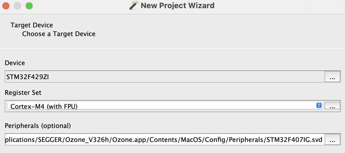
Now, run Ozone. Choose our device in the wizard:
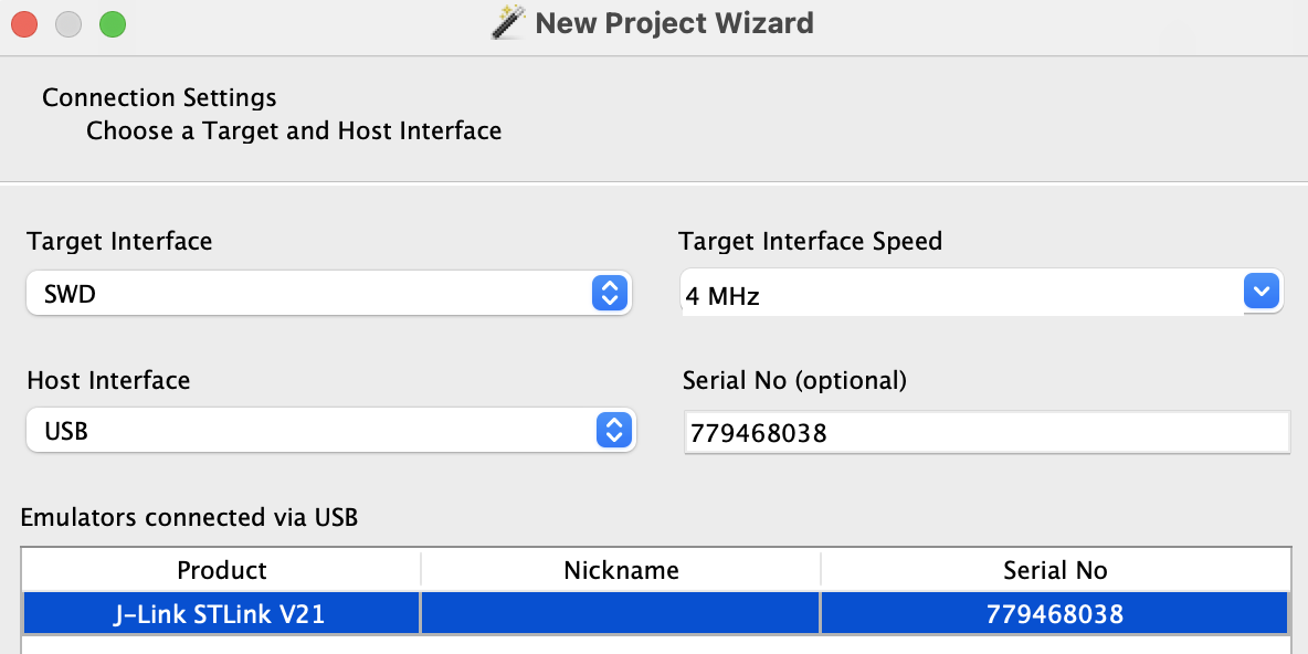
Select a debugger we're going to use - that should be a ST-LINK:
Choose our firmware.elf file:
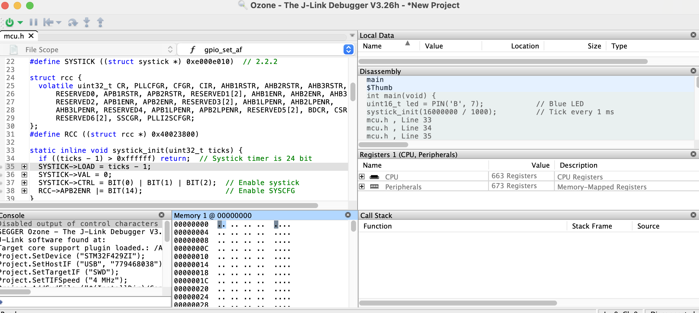
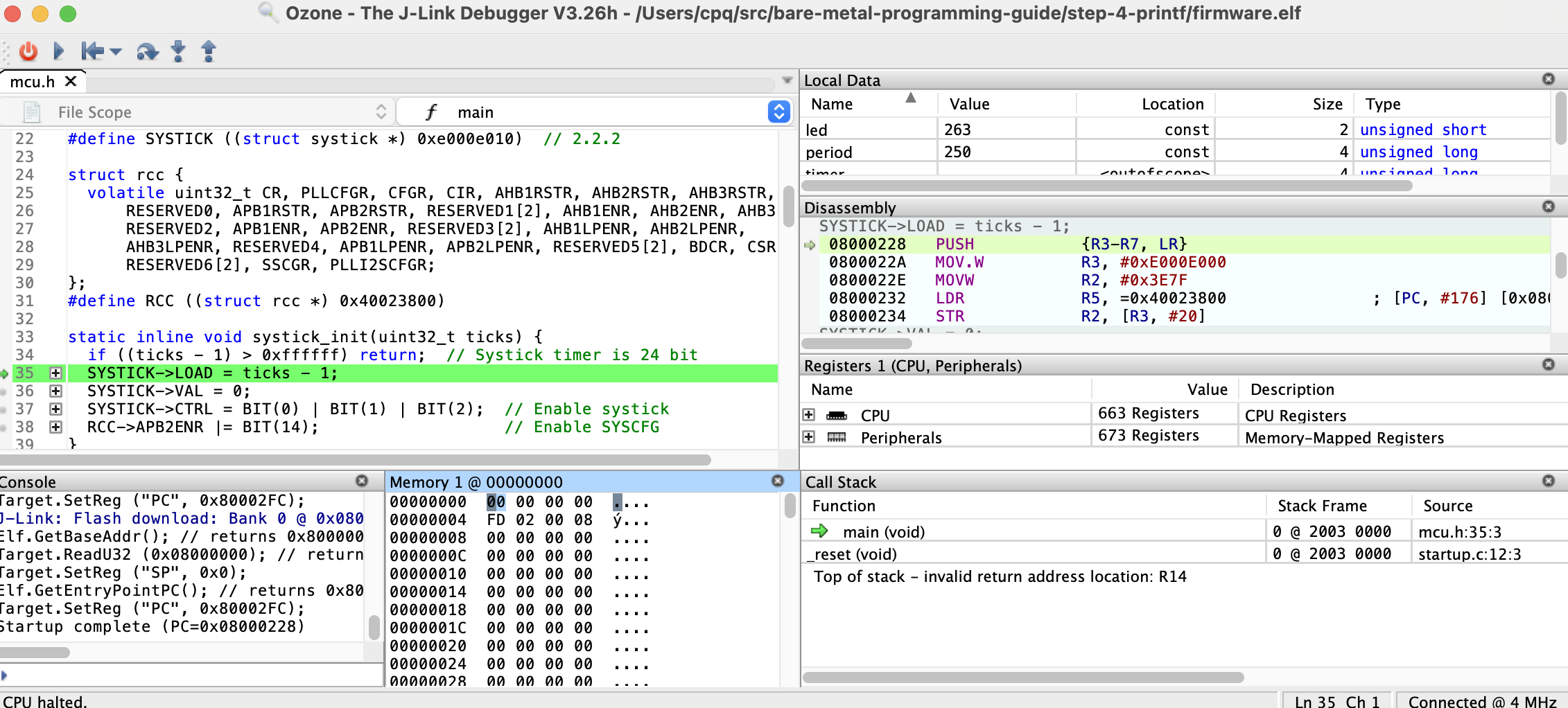
Leave the defaults on the next screen, click Finish, and we've got our debugger loaded (note the mcu.h source code is picked up):
Click the green button to download, run the firmware, and we're stopped here:
Now we can single-step through code, set breakpoints, and do the usual debugging stuff. One thing that could be noted, is a handy Ozone peripheral view:
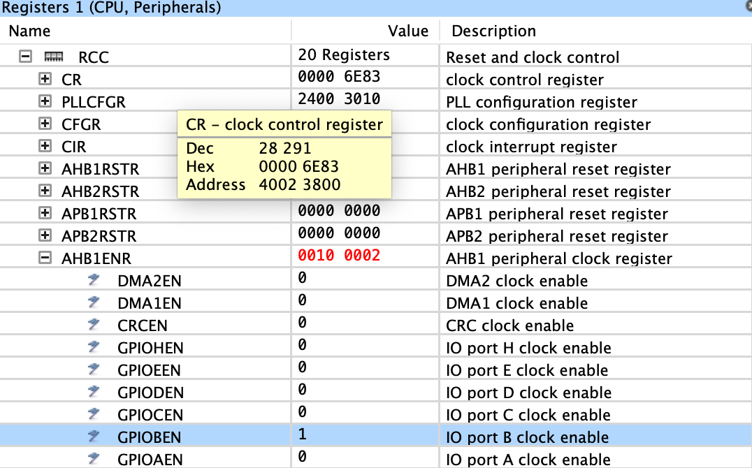
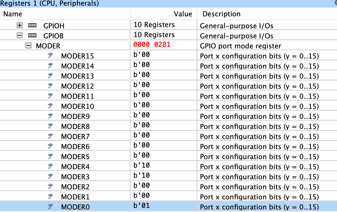
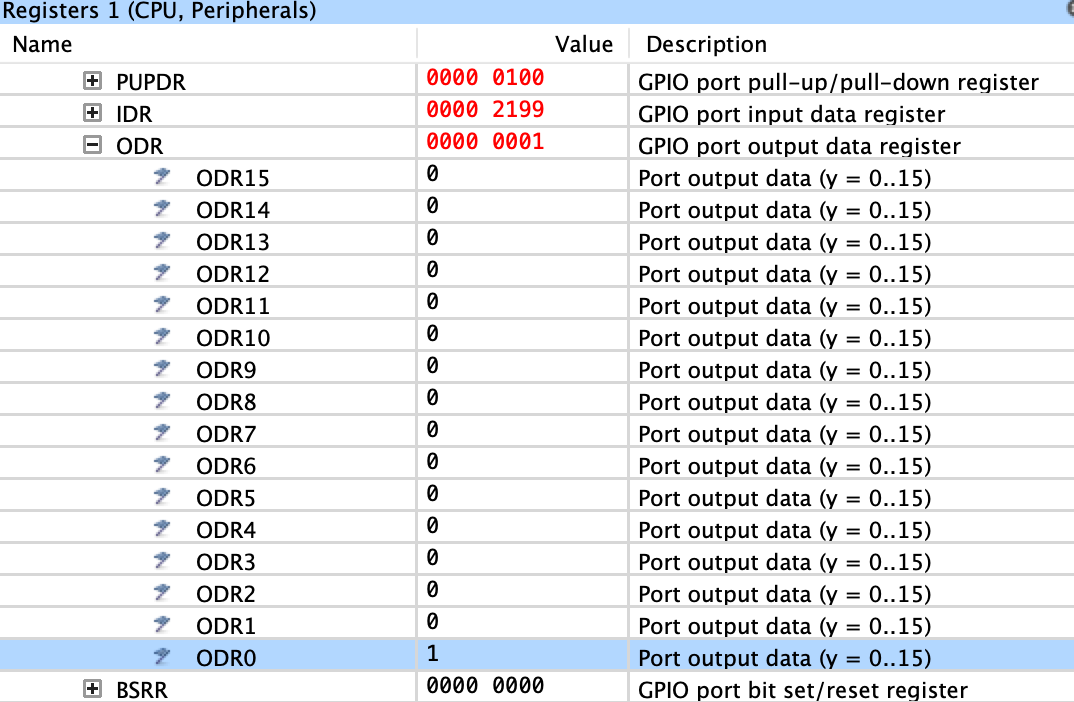
Using it, we can directly examine or set the state of the peripherals. For example, let's turn on a green on-board LED (PB0):
- We need to clock GPIOB first. Find Peripherals -> RCC -> AHB1ENR, and enable GPIOBEN bit - set it to 1:
Now, a green LED should be on! Happy debugging.
In the previous sections, we have developed the firmware using only datasheets, editor, and GCC compiler. We have created peripheral structure definitions manually, using datasheets.
Now as you know how it all works, it is time to introduce CMSIS headers. What is it ? These are header files with all definitions, created and supplied by the MCU vendor. They contain definitions for everything that MCU contains, therefore they rather big.
CMSIS stands for Common Microcontroller Software Interface Standard, thus it is a common ground for the MCU manufacturers to specify peripheral API. Since CMSIS is an ARM standard, and since CMSIS headers are supplied by the MCU vendor, they are the source of authority. Therefore, using vendor headers is is a preferred way, rather than writing definitions manually.
In this section, we will replace our API functions in the mcu.h by the
CMSIS vendor header, and leave the rest of the firmware intact.
STM32 CMSIS headers for F4 family can be found at https://github.com/STMicroelectronics/cmsis_device_f4 repo. From there, copy the following files into our firmware directory, step-5-cmsis:
Those two files depend on a standard ARM CMSIS includes, download them too:
From the mcu.h, remove all peripheral API and definitions, and leave only
standard C inludes, vendor CMSIS include, defines to PIN, BIT, FREQ, and
timer_expired() helper function:
#pragma once

#include <inttypes.h>
#include <stdbool.h>
#include <stdlib.h>
#include <stdio.h>
#include <sys/stat.h>

#include "stm32f429xx.h"

#define FREQ 16000000  // CPU frequency, 16 Mhz
#define BIT(x) (1UL << (x))
#define PIN(bank, num) ((((bank) - 'A') << 8) | (num))
#define PINNO(pin) (pin & 255)
#define PINBANK(pin) (pin >> 8)

static inline void spin(volatile uint32_t count) {
  while (count--) (void) 0;
}

static inline bool timer_expired(uint32_t *t, uint32_t prd, uint32_t now) {
  ...
}
If we try to rebuild the firmware - make clean build, then GCC will fail
complaining about missing systick_init(), GPIO_MODE_OUTPUT, uart_init(),
and UART3. Let's add those using STM32 CMSIS files.
Let's start from systick_init(). The core_cm4.h header defines
SysTick_Type structure which is identical to our struct systick, and has
an appropriate #define for SysTick peripheral. Also, stm32f429xx.h has
a RCC_TypeDef structure and appropriate #define for the RCC. Therefore
our systick_init() function remains almost unchanged: we only have to replace
SYSTICK with SysTick:
static inline void systick_init(uint32_t ticks) {
  if ((ticks - 1) > 0xffffff) return;  // Systick timer is 24 bit
  SysTick->LOAD = ticks - 1;
  SysTick->VAL = 0;
  SysTick->CTRL = BIT(0) | BIT(1) | BIT(2);  // Enable systick
  RCC->APB2ENR |= BIT(14);                   // Enable SYSCFG
}
Next goes gpio_set_mode() function. The stm32f429xx.h header has
GPIO_TypeDef structure, identical to our struct gpio. Let's use it:
#define GPIO(bank) ((GPIO_TypeDef *) (GPIOA_BASE + 0x400 * (bank)))
enum { GPIO_MODE_INPUT, GPIO_MODE_OUTPUT, GPIO_MODE_AF, GPIO_MODE_ANALOG };

static inline void gpio_set_mode(uint16_t pin, uint8_t mode) {
  GPIO_TypeDef *gpio = GPIO(PINBANK(pin));  // GPIO bank
  int n = PINNO(pin);                      // Pin number
  RCC->AHB1ENR |= BIT(PINBANK(pin));       // Enable GPIO clock
  gpio->MODER &= ~(3U << (n * 2));         // Clear existing setting
  gpio->MODER |= (mode & 3) << (n * 2);    // Set new mode
}
The gpio_set_af() and gpio_write() functions is also trivial -
simply replace struct gpio with GPIO_TypeDef, and that's all.
Next goes UART. There is a USART_TypeDef, and defines for USART1, USART2,
USART3. Let's use them:
#define UART1 USART1
#define UART2 USART2
#define UART3 USART3
In the uart_init() and the rest of UART functions, change struct uart to
USART_TypeDef. The rest stays the same!
And we are done. Rebuild, reflash the firmware. The LED blinks, the UART
shows the output. Congratulations, we have adopted our firmware code to
use vendor CMSIS header files. Now let's reorganise the repository a bit
by moving all standard files into include directory and updating Makefile
to let GCC know about it:
...
  -g3 -Os -ffunction-sections -fdata-sections -I. -Iinclude \
We have left with a project template that can be reused for the future projects. A complete project source code you can find in step-5-cmsis
After boot, Nucleo-F429ZI CPU runs at 16MHz. The maximum frequency is 180MHz. Note that system clock frequency is not the only factor we need to care about. Peripherals are attached to different buses, APB1 and APB2 which are clocked differently. Their clock speeds are configured by the frequency prescaler values, set in the RCC. The main CPU clock source can also be different - we can use either an external crystal oscillator (HSE) or an internal oscillator (HSI). In our case, we'll use HSI.
When CPU executes instructions from flash, a flash read speed (which is around
25MHz) becomes a bottleneck if CPU clock gets higher. There are several tricks
that can help. Instruction prefetch is one. Also, we can give a clue to the
flash controller, how faster the system clock is: that value is called flash
latency. For 180MHz system clock, the FLASH_LATENCY value is 5. Bits 8 and 9
in the flash controller enable instruction and data caches:
FLASH->ACR |= FLASH_LATENCY | BIT(8) | BIT(9); // Flash latency, cachesThe clock source (HSI or HSE) goes through a piece of hardware called PLL, which multiplies source frequency by a certain value. Then, a set of frequency dividers are used to set the system clock and APB1, APB2 clocks. In order to obtain the maximum system clock of 180MHz, multiple values of PLL dividers and APB prescalers are possible. Section 6.3.3 of the datasheet tells us the maximum values for APB1 clock: <= 45MHz, and the APB2 clock: <= 90MHz. That narrows down the list of possible combinations. Here we chose the values manually. Note that tools like CubeMX can automate the process and make it easy and visual.
enum { APB1_PRE = 5 /* AHB clock / 4 */, APB2_PRE = 4 /* AHB clock / 2 */ };
enum { PLL_HSI = 16, PLL_M = 8, PLL_N = 180, PLL_P = 2 };  // Run at 180 Mhz
#define PLL_FREQ (PLL_HSI * PLL_N / PLL_M / PLL_P)
#define FREQ (PLL_FREQ * 1000000)
Now we're ready for a simple algorithm to set up the clock for CPU and peripheral buses may look like this:
- Optionally, enable FPU
- Set flash latency
- Decide on a clock source, and PLL, APB1 and APB2 prescalers
- Configure RCC by setting respective values:
static inline void clock_init(void) {                 // Set clock frequency
  SCB->CPACR |= ((3UL << 10 * 2) | (3UL << 11 * 2));  // Enable FPU
  FLASH->ACR |= FLASH_LATENCY | BIT(8) | BIT(9);      // Flash latency, caches
  RCC->PLLCFGR &= ~((BIT(17) - 1));                   // Clear PLL multipliers
  RCC->PLLCFGR |= (((PLL_P - 2) / 2) & 3) << 16;      // Set PLL_P
  RCC->PLLCFGR |= PLL_M | (PLL_N << 6);               // Set PLL_M and PLL_N
  RCC->CR |= BIT(24);                                 // Enable PLL
  while ((RCC->CR & BIT(25)) == 0) spin(1);           // Wait until done
  RCC->CFGR = (APB1_PRE << 10) | (APB2_PRE << 13);    // Set prescalers
  RCC->CFGR |= 2;                                     // Set clock source to PLL
  while ((RCC->CFGR & 12) == 0) spin(1);              // Wait until done
}
What is left, is to call clock_init() from main, then rebuild and reflash.
And our board runs at its maximum speed, 180MHz!
A complete project source code you can find in step-6-clock
The Nucleo-F429ZI comes with Ethernet on-board. Ethernet hardware needs two components: a PHY (which transmits/receives electrical signals to the media like copper, optical cable, etc) and MAC (which drives PHY controller). On our Nucleo, the MAC controller is built-in, and the PHY is external (specifically, is is Microchip's LAN8720a).
MAC and PHY can talk several interfaces, we'll use RMII. For that, a bunch of pins must be configured to use their Alternative Function (AF). To implement a web server, we need 3 software components:
- a network driver, which sends/receives Ethernet frames to/from MAC controller
- a network stack, that parses frames and understands TCP/IP
- a network library that understands HTTP
We will use Mongoose Network Library which implements all of that in a single file. It is a dual-licensed library (GPLv2/commercial) that was designed to make network embedded development fast and easy.
So, copy mongoose.c and mongoose.h to our project. Now we have a driver, a network stack, and a library at hand. Mongoose also provides a large set of examples, and one of them is a device dashboard example. It implements lots of things - like dashboard login, real-time data exchange over WebSocket, embedded file system, MQTT communication, etcetera. So let's use that example. Copy two extra files:
- net.c - implements dashboard functionality
- packed_fs.c - contains HTML/CSS/JS GUI files
What we need is to tell Mongoose which functionality to enable. That can
be done via compilation flags, by setting preprocessor constants. Alternatively,
the same constants can be set in the mongoose_custom.h file. Let's go
the second way. Create mongoose_custom.h file with the following contents:
#pragma once
#define MG_ARCH MG_ARCH_NEWLIB
#define MG_ENABLE_MIP 1
#define MG_ENABLE_PACKED_FS 1
#define MG_IO_SIZE 512
#define MG_ENABLE_CUSTOM_MILLIS 1
Now it's time to add some networking code to main.c. We #include "mongoose.c",
initialise Ethernet RMII pins and enable Ethernet in the RCC:
  uint16_t pins[] = {PIN('A', 1),  PIN('A', 2),  PIN('A', 7),
                     PIN('B', 13), PIN('C', 1),  PIN('C', 4),
                     PIN('C', 5),  PIN('G', 11), PIN('G', 13)};
  for (size_t i = 0; i < sizeof(pins) / sizeof(pins[0]); i++) {
    gpio_init(pins[i], GPIO_MODE_AF, GPIO_OTYPE_PUSH_PULL, GPIO_SPEED_INSANE,
              GPIO_PULL_NONE, 11);
  }
  nvic_enable_irq(61);                          // Setup Ethernet IRQ handler
  RCC->APB2ENR |= BIT(14);                      // Enable SYSCFG
  SYSCFG->PMC |= BIT(23);                       // Use RMII. Goes first!
  RCC->AHB1ENR |= BIT(25) | BIT(26) | BIT(27);  // Enable Ethernet clocks
  RCC->AHB1RSTR |= BIT(25);                     // ETHMAC force reset
  RCC->AHB1RSTR &= ~BIT(25);                    // ETHMAC release reset
Mongoose's driver uses Ethernet interrupt, thus we need to update startup.c
and add ETH_IRQHandler to the vector table. Let's reorganise vector table
definition in startup.c in a way that does not require any modification
to add an interrupt handler function. The idea is to use a "weak symbol"
concept.
A function can be marked "weak" and it works like a normal function. The difference comes when a source code defines a function with the same name elsewhere. Normally, two functions with the same name make a build fail. However if one function is marked weak, then a build succeeds and linker selects a non-weak function. This gives an ability to provide a "default" function in a boilerplate, with an ability to override it by simply creating a function with the same name elsewhere in the code.
Here how it works in our case. We want to fill a vector table with default
handlers, but give user an ability to override any handler. For that, we create
a function DefaultIRQHandler() and mark it weak. Then, for every IRQ handler,
we declare a handler name and make it an alias to DefaultIRQHandler():
void __attribute__((weak)) DefaultIRQHandler(void) {
  for (;;) (void) 0;
}
#define WEAK_ALIAS __attribute__((weak, alias("DefaultIRQHandler")))

WEAK_ALIAS void NMI_Handler(void);
WEAK_ALIAS void HardFault_Handler(void);
WEAK_ALIAS void MemManage_Handler(void);
...
__attribute__((section(".vectors"))) void (*tab[16 + 91])(void) = {
    0, _reset, NMI_Handler, HardFault_Handler, MemManage_Handler,
    ...
Now, we can define any IRQ handler in our code, and it will replace the default
one. This is what happens in our case: there is a ETH_IRQHandler() defined
by the Mongoose's STM32 driver which replaces a default handler.
The next step is to initialise Mongoose library: create an event manager, setup network driver, and start a listening HTTP connection:
  struct mg_mgr mgr;        // Initialise Mongoose event manager
  mg_mgr_init(&mgr);        // and attach it to the MIP interface
  mg_log_set(MG_LL_DEBUG);  // Set log level

  struct mip_driver_stm32 driver_data = {.mdc_cr = 4};  // See driver_stm32.h
  struct mip_if mif = {
      .mac = {2, 0, 1, 2, 3, 5},
      .use_dhcp = true,
      .driver = &mip_driver_stm32,
      .driver_data = &driver_data,
  };
  mip_init(&mgr, &mif);
  extern void device_dashboard_fn(struct mg_connection *, int, void *, void *);
  mg_http_listen(&mgr, "http://0.0.0.0", device_dashboard_fn, &mgr);
  MG_INFO(("Init done, starting main loop"));
What is left, is to add a mg_mgr_poll() call into the main loop.
Now, add mongoose.c, net.c and packed_fs.c files to the Makefile.
Rebuild, reflash the board. Attach a serial console to the debug output,
observe that the board obtains an IP address over DHCP:
847 3 mongoose.c:6784:arp_cache_add     ARP cache: added 0xc0a80001 @ 90:5c:44:55:19:8b
84e 2 mongoose.c:6817:onstatechange     READY, IP: 192.168.0.24
854 2 mongoose.c:6818:onstatechange            GW: 192.168.0.1
859 2 mongoose.c:6819:onstatechange            Lease: 86363 sec
LED: 1, tick: 2262
LED: 0, tick: 2512
Fire up a browser at that IP address, and get a working dashboard, with real-time graph over WebSocket, with MQTT, authentication, and other things! See full description for more details.
A complete project source code you can find in step-7-webserver directory.
It is a good practice for a software project to have continuous integration (CI). On every change pushed to the repository, CI automatically rebuilds and tests all components.
Github makes it easy to do. We can create a .github/workflows/test.yml file
which is a CI configuration file. In that file, we can install ARM GCC
and run make in every example directory to build respective firmwares.
Long story short! This tells Github to run on every repo push: https://github.com/cpq/bare-metal-programming-guide/blob/b0820b5c62b74a9b4456854feb376cda8cde4ecd/.github/workflows/test.yml#L1-L2
This installs ARM GCC compiler: https://github.com/cpq/bare-metal-programming-guide/blob/b0820b5c62b74a9b4456854feb376cda8cde4ecd/.github/workflows/test.yml#L9
This builds a firmware in every example directory: https://github.com/cpq/bare-metal-programming-guide/blob/b0820b5c62b74a9b4456854feb376cda8cde4ecd/.github/workflows/test.yml#L10-L18
That's it! Extremely simple and extremely powerful. Now if we push a change to the repo which breaks a build, Github will notify us. On success, Github will keep quiet. See an example successful run.
Would it be great to also test built firmware binaries on a real hardware, to test not only the build process, but that the built firmware is correct and functional?
It is not trivial to build such a system ad hoc. For example, one can setup a dedicated test workstation, attach a tested device (e.g. Nucleo-F429ZI board) to it, and write a piece of software for remote firmware upload and test using a built-in debugger. Possible, but fragile, consumes a lot of efforts and needs a lot of attention.
The alternative is to use one of the commercial hardware test systems (or EBFs, Embedded Board Farms), though such commercial solutions are quite expensive.
But there is an easy way.
Using https://vcon.io service, which implements remote firmware update and UART monitor, we can:
- Take any ESP32 or ESP32C3 device (e.g. any inexpensive development board)
- Flash a pre-built firmware on it, turning ESP32 into a remotely-controlled programmer
- Wire ESP32 to your target device: SWD pins for flashing, UART pins for capturing output
- Configure ESP32 to register on https://dash.vcon.io management dashboard
When done, your target device will have an authenticated, secure RESTful API for reflashing and capturing device output. It can be called from anywhere, for example from the software CI:
Note: the vcon.io service is run by Cesanta - the company I work for. It is a paid service with a freebie quota: if you have just a few devices to manage, it is completely free.
Take any ESP32 or ESP32C3 device - a devboard, a module, or your custom device. Our recommendation is ESP32C3 XIAO devboard (buy on Digikey) because of its low price (about 5 EUR) and small form factor.
We're going to assume that the target device is a Raspberry Pi W5500-EVB-Pico board with a built-in Ethernet interface. If your device is different, adjust the "Wiring" step according to your device's pinout.
- Follow Flashing ESP32 to flash your ESP32
- Follow Network Setup to register ESP32 on https://dash.vcon.io
- Follow Wiring to wire ESP32 to your device
This is how a configured device breadboard setup may look like:
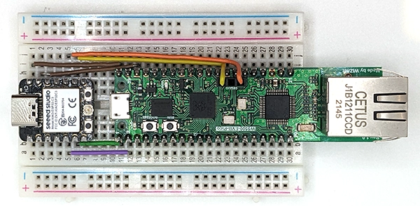
This is how a configured device dashboard looks like:
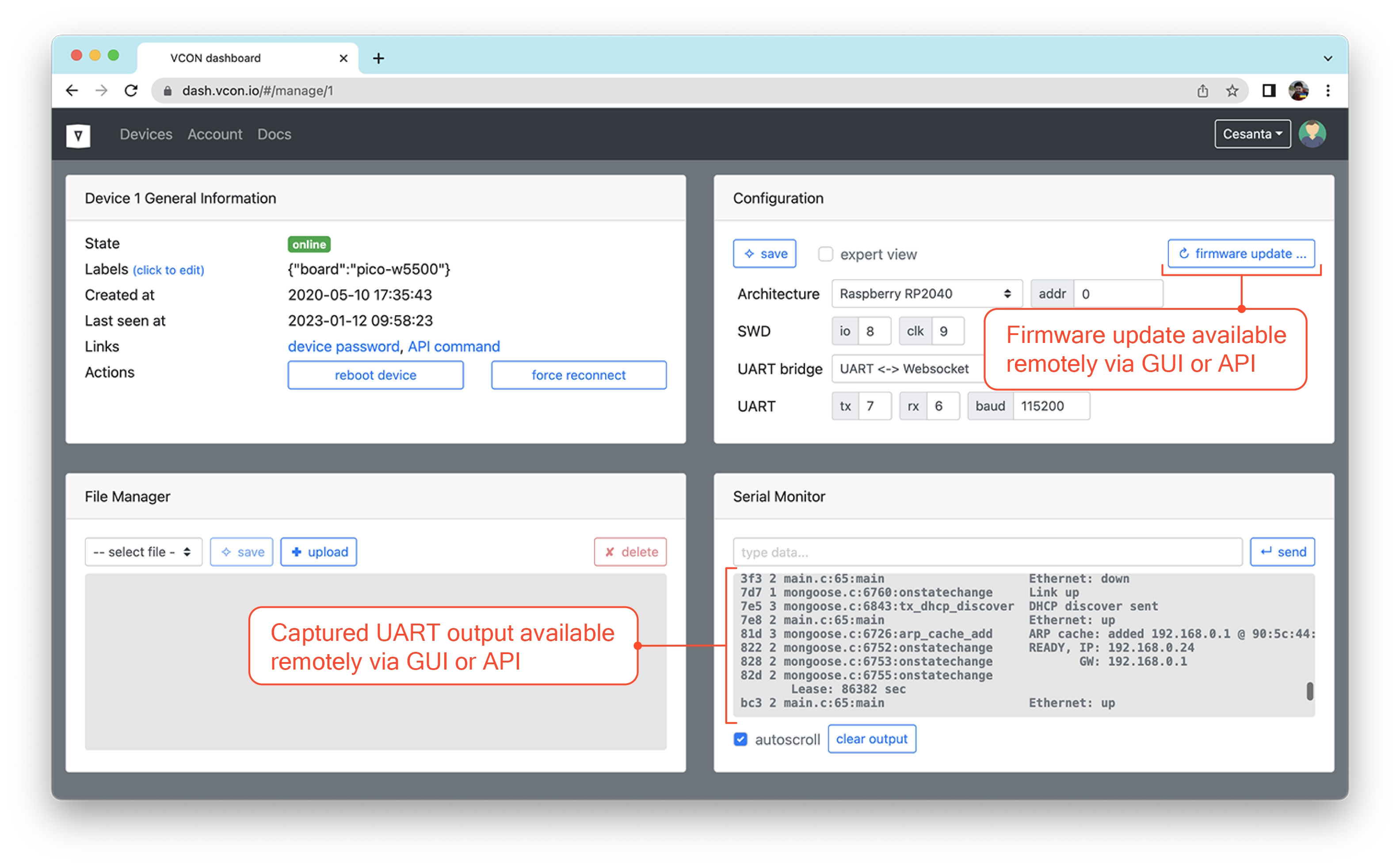
Now, you can reflash your device with a single command:
curl -su :$API_KEY 'https://dash.vcon.io/api/v3/devices/$ID/ota' --data-binary @firmware.binWhere API_KEY is the dash.vcon.io authentication key, ID is the registered
device number, and firmware.bin is the name of the newly built firmware. You
can get the API_KEY by clicking on the "api key" link on a dashboard. The
device ID is listed in the table.
We can also capture device output with a single command:
curl -su :$API_KEY 'https://dash.vcon.io/api/v3/devices/$ID/tx?t=5'There, t=5 means wait 5 seconds while capturing UART output.
Now, we can use those two commands in any software CI platform to test a new firmware on a real device, and test device's UART output against some expected keywords.
Okay, our software CI builds a firmware image for us. It would be nice to
test that firmware image on a real hardware. And now we can!
We should add few extra commands that use curl utility to send a built
firmware to the test board, and then capture its debug output.
A curl command requires a secret API key, which we do not want to expose to
the public. The right way to go is to:
- Go to the project settings / Secrets / Actions
- Click on "New repository secret" button
- Give it a name,
VCON_API_KEY, paste the value into a "Secret" box, click "Add secret"
One of the example projects builds firmware for the RP2040-W5500 board, so
let's flash it using a curl command and a saved API key. The best way is
to add a Makefile target for testing, and let Github Actions (our software CI)
call it:
https://github.com/cpq/bare-metal-programming-guide/blob/8d419f5e7718a8dcacad2ddc2f899eb75f64271e/.github/workflows/test.yml#L18
Note that we pass a VCON_API_KEY environment variable to make. Also note
that we're invoking test Makefile target, which should build and test our
firmware. Here is the test Makefile target:
https://github.com/cpq/bare-metal-programming-guide/blob/d9bced31b1ccde8eca4d6dc38440e104dba053ce/step-7-webserver/pico-w5500/Makefile#L32-L39
Explanation:
- line 34: The
testtarget depends on theuploadtarget, souploadis executed first (see line 38) - line 35: Capture UART log for 5 seconds and save it to
/tmp/output.txt - line 36: Search for the string
Ethernet: upin the output, and fail if it is not found - line 38: The
uploadtarget depends onbuild, so we always build firmware before testing - line 39: We flash firmware remotely. The
--failflag tocurlutility makes it fail if the response from the server is not successful (not HTTP 200 OK)
This is the example output of the make test command described above:
$ make test
curl --fail ...
{"success":true,"written":59904}
curl --fail ...
3f3 2 main.c:65:main                    Ethernet: down
7d7 1 mongoose.c:6760:onstatechange     Link up
7e5 3 mongoose.c:6843:tx_dhcp_discover  DHCP discover sent
7e8 2 main.c:65:main                    Ethernet: up
81d 3 mongoose.c:6726:arp_cache_add     ARP cache: added 192.168.0.1 @ 90:5c:44:55:19:8b
822 2 mongoose.c:6752:onstatechange     READY, IP: 192.168.0.24
827 2 mongoose.c:6753:onstatechange            GW: 192.168.0.1
82d 2 mongoose.c:6755:onstatechange            Lease: 86336 sec
bc3 2 main.c:65:main                    Ethernet: up
fab 2 main.c:65:main                    Ethernet: up
Done! Now, our automatic tests ensure that the firmware can be built, that is it bootable, that it initialises the network stack correctly. This mechanism can be easily extended: just add more complex actions in your firmware binary, print the result to the UART, and check for the expected output in the test.
Happy testing!
I am Sergey Lyubka, an engineer and entrepreneur. I hold a MSc in Physics from Kyiv State University, Ukraine. I am a director and co-founder at Cesanta - a technology company based in Dublin, Ireland. My passion is bare metal embedded network programming. My company develops embedded solutions:
- https://mongoose.ws - an open source HTTP/MQTT/Websocket network library
- https://vcon.io - a remote firmware update / serial monitor framework
I am open to give talks on embedded network programming - so please contact if you'd like me to talk for your company's development team, or at your university.
Thank you!


