- Introduction
- Installation and running the tool
- Parameters
Current Maintainers: Nihar Dasari dnihar@gatech.edu, Venkata Chaitanya Krishna Chekuri vchekuri3@gatech.edu
This tool is used to generate the PID realisation of a Switched inductor DC-DC converter and for simulation in Simulink. It can be used to generate a voltage regulator for a given bandwidth and phase margin or can automatically choose the highest bandwidth possible for a given phase margin.
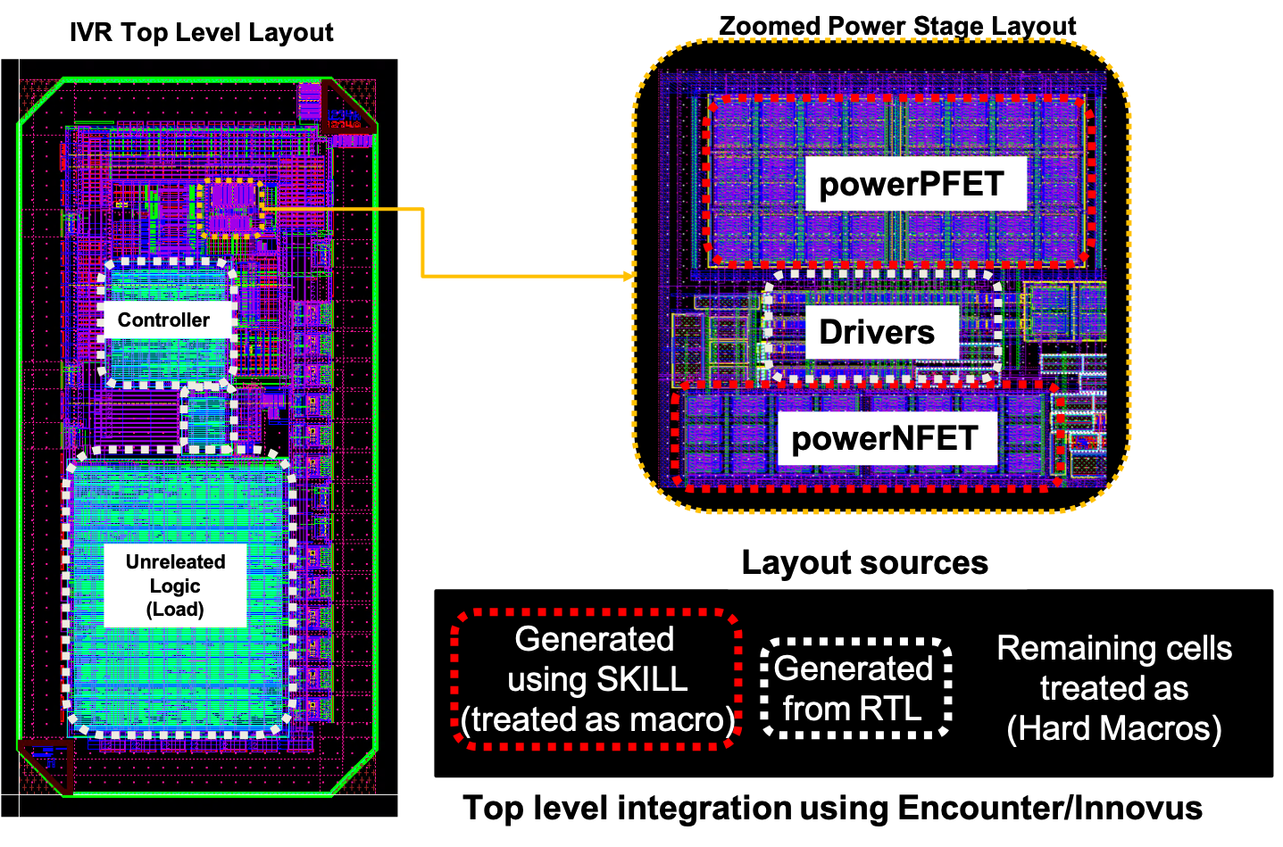
Final IVR layout should be something along the lines of the following image. The Cadence SKILL codes and Innovus tcl files will be added to this project in future.

Ther is no installation required. To use, donload the contents of the project
It should contain 5 files:
target_specs.csv
IVR.slx
ivr_specs_gen.m
calctime.m
simout.m
And 1 folder Efficiency_computation_for_buck_converter
To run, the following are required: Matlab 2016b or higher Simulink 2016 or higher
The code has been tested on versions 2016 and higher and could run on older versions, functionality is not guaranteed
To run the code, simply execute ivr_specs_gen.m while ensuring target_specs.csv and IVR.slx are present in the working directory
The target specifications for the voltage regulator are defined in target_specs.csv. These are listed below Read the target specs from target_specs.csv Format of the target_specs.csv follows
| Vin | Input voltage in volts |
|---|---|
| V_ref | Reference voltage in volts |
| ref_step_en | (1/0) Enables/Disables reference transient event |
| ref_step | Reference step in V to reach Vref (Used for reference transient simulations) |
| F_SW | Power stage/DPWM switching Frequency in Hz |
| N | Factor of F_SW by which ADC samples the voltage error. N!=1 for multisampling |
| phm_d | Target phase margin in degrees |
| Fc | Target Unity gain or crossover frequency in Hz |
| L | Output filter inductance |
| C | Output filter capacitance |
| ESR_L | Effective series resistance of output filter inductor |
| ESR_C | Effective series resistance of output filter capacitor |
| L_BW | Inducatance for the pads |
| ESR_L_BW | Effective series resistance for PAD inductance |
| C_DECAP | Input decap at pads |
| ESR_C_DECAP | Effecrtive series resistance for input decaps at pads |
| I_Load | Load current |
| ADC_lower_range | Lower range of ADC |
| ADC_higher_range | Upper Range of ADC |
| ADC_reso_bits | ADC resolution in bits |
| DPWM_reso_bits | DPWM resolution in bits |
| load_step_en | (1/0) Enables/Disables load transient event |
| I_load_init | Initial output current in A before load transient event (Used for load transient simulations) |
| load_step_time | Time in s at which load step is introduced (Used for load transient simulations) |
| load_step | Load step value in A at load_step_time (Used for load transient simulations) |
| wk0_bits | NA |
| fb_wk1_bits | NA |
| fb_wk2_bits | NA |
| fb_wk3_bits | Compensator gain |
| comp_gain | (1/0) Disables/Enables detailed log statements |
| quiet | (1/0) Enables/Disables Simulink Simulation |
| simu | (1/0) Automatically optimise for Bandwidth and phase/Use given bandwidth and phase margin targets |
| auto |