The Unified Daughterboard Project is an attempt by leading designers in the mechanical keyboard community to standardize the USB daughterboards used for their custom mechanical keyboard projects. It has initially been envisioned by users ai03, Wilba, Hineybush, Xelus, Xondat, aeryxz and Maximillian.
The main characteristic of this daughterboard is to integrate a USB Type C connector and the needed circuitry for USB2.0 operation in a small PCB that can be screwed to a keyboard chassis; this significantly simplifies the assembly and design of the main circuit board.
In its latest version, C3, this daughterboard features:
- ESD (Electrostatic Discharge) protection on the data lines of the USB connector through a specialized chip;
- Overcurrent protection through a PTC fuse;
- Overvoltage protection through a bidirectional TVS diode;
- Shielding noise decoupling capabilities through a ferrite bead;
- Single-path grounding of the metallic chassis to which the daughterboard is attached.
Adittionally, the C3 version is backwards compatible with both C1 and C2 versions since it has the same dimensions and uses the same screw hole sizes and positions, so keyboards designed using the past versions should also support C3.
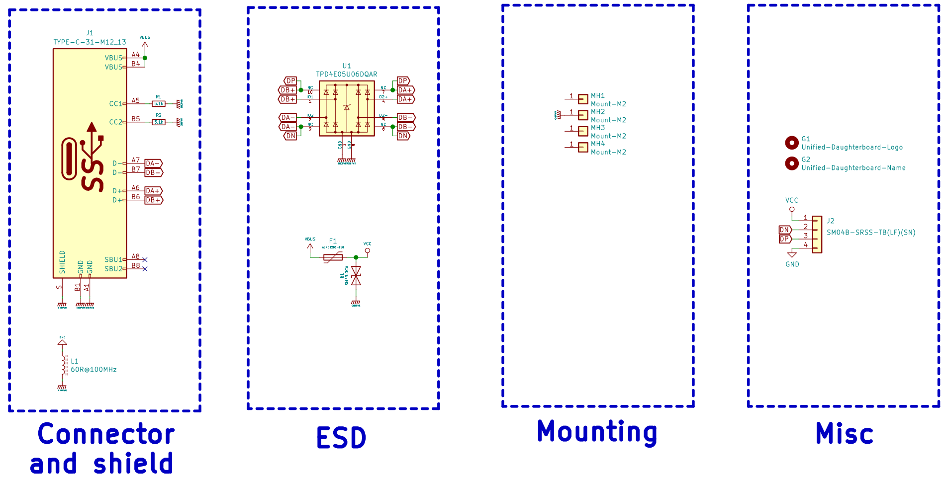
The figure below shows the schematic of the C3 version.
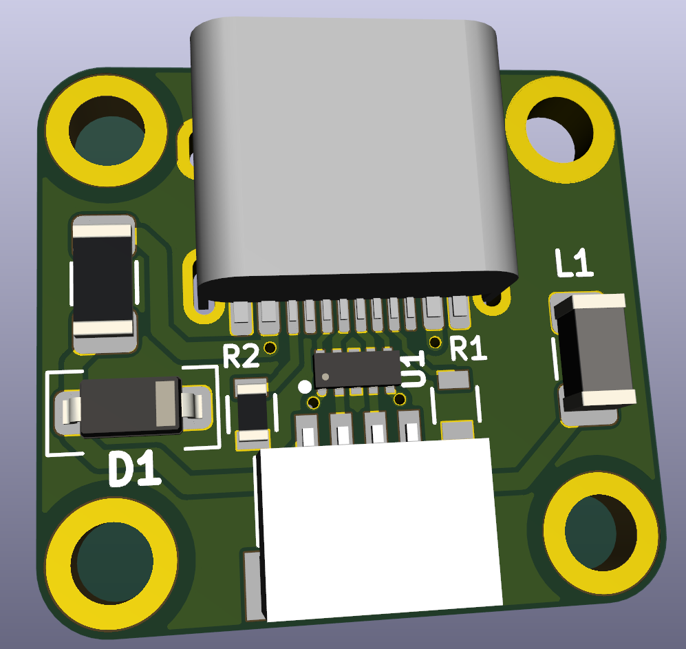
- U1 is the ESD protection for the USB data lines. It is a ultra-fast, low-capacitance chip specifically designed for USB type C connectors. When one of the data lines presents a sudden voltage spike, this chip promptly grounds it -- avoiding damage to the circuit that uses these lines;
- Resistors R1 and R2 are the CC resistors needed for operation of the USB Type C. These resistors are used by the USB host to know that the daughterboard is a downstream device and which side of the USBC connector is connected;
- Fuse F1 provides overcurrent protection. It is a PTC resettable;
- Diode D1 is a Transient Voltage Suppressor that exerpts to the power rails of the connector the same effect as the U1 chiup to data lines; when a voltge spike is detected, it shorts VCC and GND, aavoiding damage to the forward circuitry;
- Inductor L1 is a ferrite bead that presetns a very low impedance between the power ground and the signal ground in DC regimen; in high frequencies (for instance in an ESD event) it presents a very high impedance, avoiding noisy currents passing to the signal GND;
- The daughterboard features four screw holes used to fix it into a metal chassis. The top left mounting hole is shorted to the power ground signal; this means that the metal chassis of the keyboard will be grounded. However, the other three screw holes are not shorted to the power ground and are effectively isolated from that signal. This ensures that, in a discharge event emerging from the user providing charge to the system, the discharge current will have a single path through the daughterboard to the power ground; inductor L1 ensures that the discharge current is kept in the power ground plance and does not follow through to the signal ground.
- Gondolindrim
- ai03
- Wilba
- Hineybush
- Xelus
- Xondat
- aeryxz
- Maximillian
- Upas


