Licensed under Creative Commons Attribution 4.0 International.
Exceptions:
DMG-CPU-06/DMG-CPU-06.jpg,MGB-xCPU/MGB-LCPU-02.jpg: assumed to be in public domain based on the readme.txt file
Used libraries:
Quick links:
Traced based on high-res scans by Alex a.k.a. ArcadeTV.
Components were identified by desoldering and measuring everything on a DMG-CPU-06 board.
Note: there are several versions of original Game Boy mainboards, and these schematics have accurate information only for DMG-CPU-06
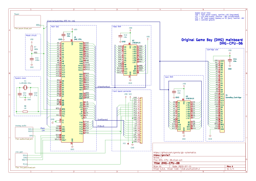
Original Game Boy mainboard schematics

Traced DMG-CPU-06 board SVG
Components were identified by desoldering and measuring everything on a DMG-LCD-06 board.
Note: there are several versions of original Game Boy LCD boards, and these schematics have accurate information only for DMG-LCD-06
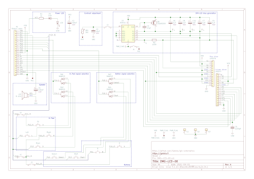
Original Game Boy LCD board (DMG-LCD-06) schematics
Components were identified by desoldering and measuring everything on one board of each type (A/B/C/D).
There are several versions of the regulator board, but the board label is not enough to distinguish the different versions. gbhwdb uses unofficial type A1/A2/A3/B/C/D designation, which is also used here. Identify your board by looking at the following board version comparison photo:

Schematics:
- DC CONV DMG (type A / type B) schematics
- DC CONV DMG (type C) schematics
- DC CONV2 DMG (type D) schematics
Visual component references:
- DC CONV DMG (type A) visual component reference
- DC CONV DMG (type B) visual component reference
- DC CONV DMG (type C) visual component reference
- DC CONV2 DMG (type D) visual component reference
Known differences:
- A1 vs A2 vs A3: one trace is laid out slightly differently at the bottom of the board
- A vs B: exactly the same circuit, but the board layout has been redone and small components now come in MicroMELF packages (vs 0603 imperial)
- B vs C: almost exactly the same circuit, but the input filter no longer has an inductor, and many component values have been slightly changed. Schottky diode switched from surface-mount SOT-23 package to through-hole DO-34.
- C vs D: main circuit and components are identical, but an extra undervoltage lockout (UVLO) circuit has been added and board layout has been redone once again

Components were identified by desoldering and measuring everything on one board of each type.
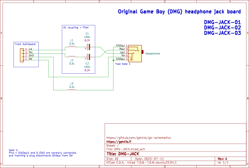
Original Game Boy headphone jack board schematics
Traced SVGs:
Traced based on high-res scans by Alex a.k.a. ArcadeTV.
Components were identified by desoldering and measuring everything on MGB-ECPU-01 and MGB-LCPU-01 boards.
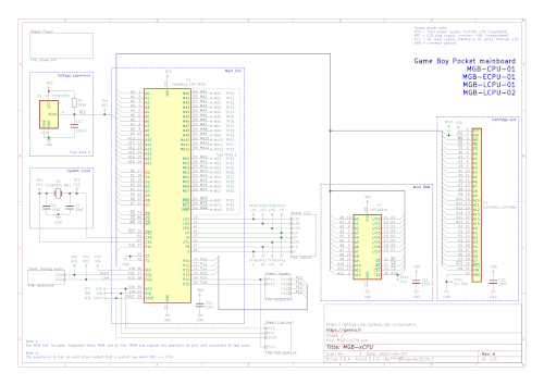
Game Boy Pocket mainboard schematics

Traced MGB-LCPU-02 board SVG
Raw notes of MGB-ECPU-01 board components
Components were identified by desoldering and measuring everything on one board of each type (A/B).
There are actually at least three different variants of this board with some minor layout adjustments, but the same schematics apply to all of them.


Components were identified by desoldering and measuring everything on an MGL-CPU-01 board.
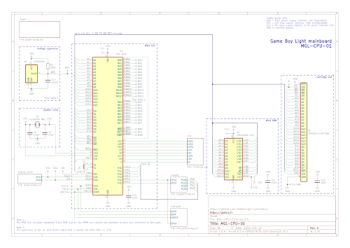
Game Boy Light mainboard schematics

Traced MGL-CPU-01 board SVG
Raw notes of MGL-CPU-01 board components
Components were identified by desoldering and measuring everything on a AGS-CPU-11 board.
Note: there are several versions of Advance SP mainboards, and these schematics have accurate information only for AGS-CPU-11
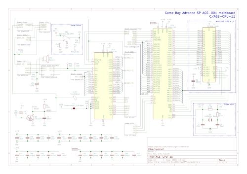
Game Boy Advance SP AGS-001 mainboard (AGS-CPU-11) schematics
Raw notes of AGS-CPU-11 board components

Traced AGS-CPU-11 board SVG