Implementation of "Enoch" Computer version 2, designed by Enoch O. Hwang, in his book Digital Logic and Microprocessor Design with VHDL, 2005.
The computer follows the Von Neumann approach, as an 8b microprocessor with internal data+instruction RAM memory, including input/output ports.
The instruction set is composed on eight different instructions:
| Instruction | Encoding | Operation | Comment |
|---|---|---|---|
| LOAD A, address | 000aaaaa | A <= Mem[aaaaa] | Load to A the memory data specified by address. |
| STORE A, address | 001aaaaa | Mem[aaaaa] <= A | Store A content to memory location specified by address |
| ADD A, address | 010aaaaa | A <= A + Mem[aaaaa] | Add A content with memory data and stores in A |
| SUB A, address | 011aaaaa | A <= A - Mem[aaaaa] | Substract A content with memory data and stores in A |
| IN A | 100----- | A <= input | Store the input data into A |
| JZ address | 101aaaaa | if (A=0) PC <= aaaaa | Jump to memory location if A content is zero |
| JPOS address | 110aaaaa | if (A>0) PC <= aaaaa | Jump to memory location if A content is positive |
| HALT | 111----- | HALT | Halts the execution of the program. |
where
- A : 8b accumulator register.
- Mem : internal 32x8b RAM memory.
- aaaaa : 5 bit address to point one of the memory slots.
- ----- : not defined nor used bits
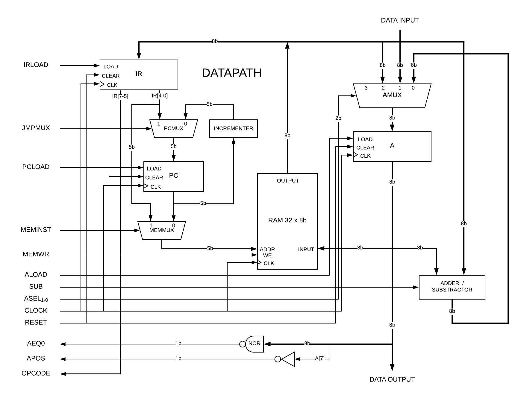
The datapath or process unit is designed based on the instruction set, because it has to perform all the functional and arithmetic operations, which are specified by the instructions. The components will be:
- A (8b) : Accumulator register. Stores the result of arithmetic operation.
- RAM memory (32x8b) : Internal memory with synchronous read and write operations.
- IR (8b) : Instruction Register, stores the current instruction fetched from memory.
- PC (5b) : Program Counter. Contains the next instruction address.
- Incrementer (5b) : Used to increment PC's content.
- Adder/Substractor (8b) : Performs addition and substraction.
- PCmux (5b) : 2-1 multiplexor which selects the next PC address.
- MEMmux (5b) : 2-1 multiplexor to select the next memory address.
- Amux (8b) : 4-1 multiplexor to select the next accumulator content.
The datapath's operations are classified on their purpose:
Instruction cycle:
- Loads the instruction from memory to IR. Increments PC content by one and load it back to PC.
- Distinguish between memory fecthing address (to fecth the next instruction) and memory operand address (to point some memory data).
Memory cycle:
- Reads the memory data/instruction specified by memory address and loads it to A/IR.
- Writes A content to the memory location specified by memory address.
Execution cycle:
- Adds or substracts to A content the memory output data, and loads the result back to A.
- Loads the external data input to A.
- Loads the operand address specified by jump instruction on PC.
The datapath also has to provide the next status signals to CU:
- Aeq0 (1b) : Tells to CU whether A content is zero. Implemented on A output with an 8b NOR gate.
- Apos (1b) : Tells to CU whether A content is positive. Implemented by negating the most significant bit of A output.
- Opcode (3b) : The three most significant bits of IR output, tells to CU which instruction to execute.
From the components and functionallity, we will need up to 8 control signals from CU, which are:
- IRload (1b) : IR load enable signal.
- JMPmux (1b) : PCMux selection signal.
- PCload (1b) : PC load enable signal.
- MEMinst (1b) : MemMux selection signal.
- MEMwr (1b) : Memory write enable signal.
- Asel (2b) : Amux selection signals.
- Aload (1b) : A load enable signal.
- Sub (1b) : substraction enable signal.
So here's the Datapath design, which best describes the conections between it's components:
We have defined all the signals to control datapath's operations. The control unit is a FSM (Finite State Machine), whose output are these control signals, grouped as a 'control word'. Each possible control word is performed in one clock cycle.
Definition of FSM states, to perform all the operations of the datapath:
-
START (0000) : The 'no operation' state. Acts as a stall, in order to load all the previous result values. Also reads from memory the next instruction pointed by PC.
-
FETCH (0001) : Fetches the available next instruction, by loading directly to IR, and increases PC by one.
-
DECODE (0010) : Transition state depending on opcode. Reads the memory content given by instruction operand address.
-
LOAD (1000) : Loads the memory available content from DECODE state to A.
-
STORE (1001) : Stores A content on the memory location given by instruction operand address.
-
ADD (1010) : Sums A content with memory available content from DECODE state, and loads the result back into A.
-
SUB (1011) : Substract A content with memory available content from DECODE state, and loads the result back into A.
-
IN (1100) : Loads 8b external data input into A.
-
JZ (1101) : If A content is zero (Aeq0 = 1), loads the instruction operand address into PC. If not, does nothing.
-
JPOS (1110) : If A content is positive (Apos = 1), loads the instruction operand address into PC. If not, does nothing.
-
HALT (1111) : Halts the execution, by only asserting the halt signal.
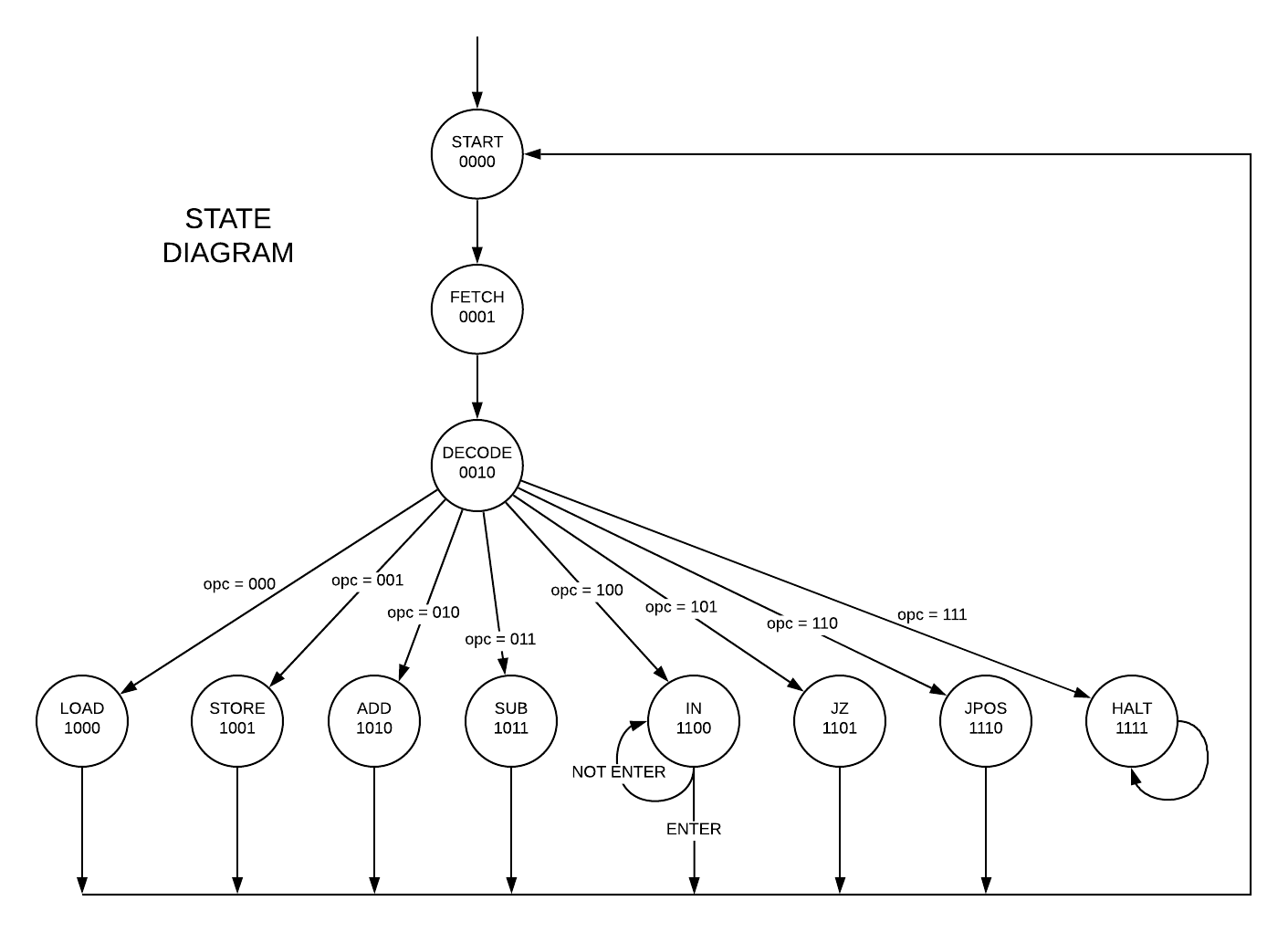
Now that all the states are defined, we can derive the state diagram, following the Moore model:
where:
- opc : operand code from Datapath's current instruction. Acts as input of the FSM.
- ENTER : external signal of CU. When asserted, the data input enters to datapath, so the transition IN => START can be done.
The control output is not defined in the state bubbles because of the space. Instead, all state's control words are described in the output table:
| CURRENT STATE | IRLOAD | JMPMUX | PCLOAD | MEMINSTR | MEMWR | ASEL | ALOAD | SUB | HALT |
|---|---|---|---|---|---|---|---|---|---|
| 0000 (start) | 0 | 0 | 0 | 0 | 0 | 00 | 0 | 0 | 0 |
| 0001 (fetch) | 1 | 0 | 1 | 0 | 0 | 00 | 0 | 0 | 0 |
| 0010 (decode) | 0 | 0 | 0 | 1 | 0 | 00 | 0 | 0 | 0 |
| 1000 (load) | 0 | 0 | 0 | 0 | 0 | 10 | 1 | 0 | 0 |
| 1001 (store) | 0 | 0 | 0 | 1 | 1 | 00 | 0 | 0 | 0 |
| 1010 (add) | 0 | 0 | 0 | 0 | 0 | 00 | 1 | 0 | 0 |
| 1011 (sub) | 0 | 0 | 0 | 0 | 0 | 00 | 1 | 1 | 0 |
| 1100 (in) | 0 | 0 | 0 | 0 | 0 | 01 | 1 | 0 | 0 |
| 1101 (jz) | 0 | 1 | Aeq0 | 0 | 0 | 00 | 0 | 0 | 0 |
| 1110 (jpos) | 0 | 1 | Apos0 | 0 | 0 | 00 | 0 | 0 | 0 |
| 1111 (halt) | 0 | 0 | 0 | 0 | 0 | 00 | 0 | 0 | 1 |
For example, when reaching START state, the control unit will be outputting zeros for each control signal until next clock's active edge, when the transition START => FETCH state is done.
Because of the VHDL behavioral style, is not necessary to build the structural design of CU, unlike Datapath's design. Then, the processor VHDL code follows a FSM+D model. That means we build the Datapath and the CU on separated entites, and then we plug both inside a top-level entity, called microprocessor, where the control and status signals connections are made.
The complete circuit design of the processor is like this one:
The VHDL attached files contain the entity we're emulating and its architecture. These are:
- reg.vhdl : Generic bit width register. Behavioral architecture.
- mux2_1.vhdl : Generic bit width 2_1 multiplexor. Behavioral architecture.
- mux4_1.vhdl : Generic bit width 4_1 multiplexor. Behavioral architecture.
- add_sub.vhdl : Generic bit width adder/substractor. Behavioral architecture.
- incrementer.vhdl : Generic bit width incrementer. Behavioral architecture.
- memory.vhdl : 32x8b memory with synchronous read/write operations. Behavioral architecture.
- datapath.vhdl : Implementation of Datapath design. Composed of all the components previosly specified. RTL architecture.
- controller.vhdl : Implementation of Controller design. Based on two main processes, next_state_logic, and output_logic. Behavioral architecture
- microprocessor.vhdl : Implementation of the complete circuit design. Has two main components, the CU and the Datapath. RTL architecture.
and two VHDL files for testing, which are:
- microprocessor_tb.vhdl : Contains the testbench entity and body test.
- microprocessor_tb_conf.vhdl : Contains the testbench configuration.
For the processor to run a program, it has to be charged directly on memory initiallization, in the memory.vhdl file. Then, running the testbench will generate the input/output signals of the processor, called EC2.
These input signals include an 8b data input signal, clock signal, reset signal, and Enter signal. The reset (active high) signal clears all Datapath's registers, and changes the CU state to START state, asynchronously. When the signal goes down, the processor will start the execution beginning with the 00h memory instruction, and passing through different states until HALT is reached. The Enter signal is used for entering data input, whenever we reach the IN state. If not asserted, the execution will stop at this state, waiting for input to be read.
The output signals include the halt signal, asserted once the HALT state is reached, and an 8b data output. This last signal will be always available, as no tri-state buffer is used.
The VHDL files can be compiled in the order given above. To run the test, I used to type: ghdl -r --workdir=work test_conf --vcd=waves.vcd and then halt it with cntr+C. This will generate a vcd file that can be visualized with some waveform application.
Finally, I've included four instruction programs in the programs.vhdl file. By default, the memory is initialized with INPUT_PRODUCT program, which performs the product of input signal values.


