(Supplemented by notebook for basic notes and ideas)
Pt. 1: Hardware Build HACK computer Silicon to low level code
    elementary logic units (NAND2 to DMUX8Way)
    |
    ALU (Half Adders to ALU)
    |
    Registers and Memory (Bit Memory to Program Counter)
    |
    Computer Architecture (Memory > CPU > Computer)
    |
    Low Level Programs
    |
    Assembler
Pt. 2: Software Create full SW hierarchy to run Tetris Low level code to Tetris
Abstraction Layers!
NAND2: y = a' * b'
    a   b   y
    0   0   1
    0   1   1
    1   0   1
    1   1   0
/** Comments here **/

CHIP Xor {
    in a, b;
    out out;
    // =========================== interface ^
    // Must specify input first then output

/* First breakdown the truth table you want to implement into all the wires that make it up.
    For instance, xXORy = x'y + xy' which means:
        The out is connected to an OR gate with inputs x'y and xy'
        The out_x'y is connected to an AND gate with inputs x' and y
        The out_xy' is connected to an AND gate with inputs x and y'
        The the out_x' is connected to a NOT gate with input x
        The the out_y' is connected to a NOT gate with input y

        Once you get to the primitive wires, stop and work backwards
        Needed wires: notx, noty, xy', x'y

    (we're using a, b, and out instead of x and y...) **/


    PARTS:
        Not (in=a, out=nota);
        Not (in=b, out=notb);

        And (a=nota, b=b, out=notaAndb);
        And (a=a, b=notb, out=aAndNotb);

        Or (a=aAndNotB, b=notaAndb, out=out);

    // =========================== implementation ^
}
HDL has infinite FANOUT; meaning it can output any number of a wire instantaneously. (No driving requirements!)
Gate implementation convention: function(a=first_input, b=second_input, ..., out=final_output)
To verify the values of internal and external outputs. Script based simulation:
load file_to_be_tested.hdl;
output-file output_of_test.out;
set a 0, set b 0, eval, output;
set a 0, set b 1, eval, output;
set a 1, set b 0, eval, output;
set a 1, set b 1, eval, output;
Comparing our output file to a predefined goal file makes testing the performance of our chip less overwhelming for chips with a large number of inputs.
Add this section to your test file along with the pre-populated truth table:
compare-to output-expectations.cmp,
after selecting the output file on the second line (don't separate the lines with a semicolon, just a comma).
Think of a group of bits as a single entity called a bus. In HDL, buses are handled by ___________
For instance, a 16-bit adder gets treated like 2 16-bit numbers are going into it instead of 32 individual lines carrying a sigle bit each.
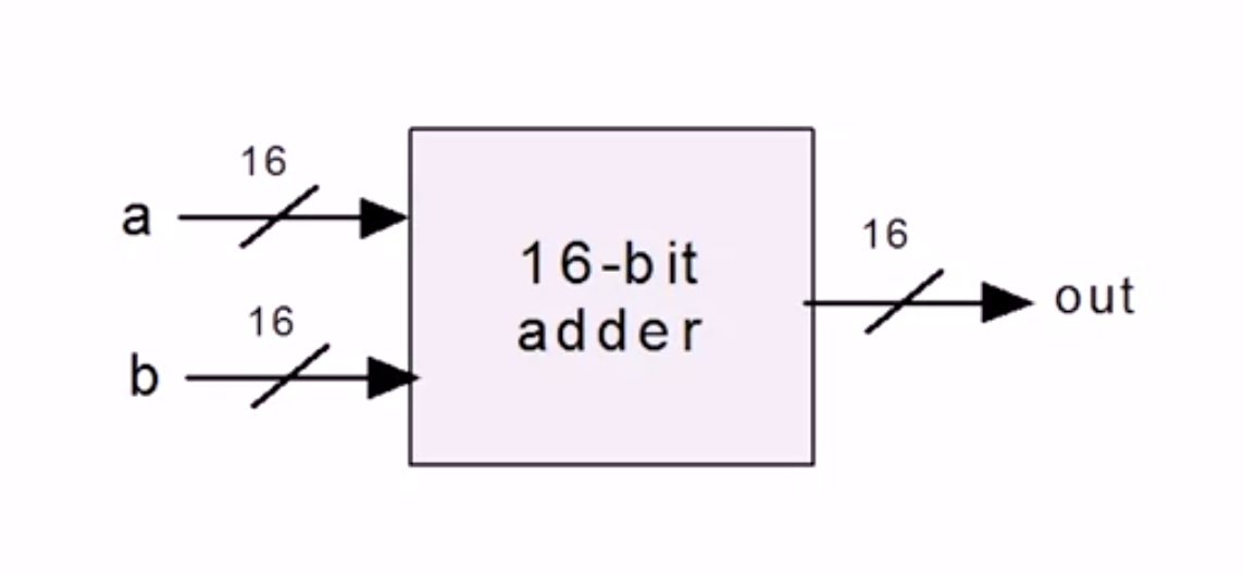
Skeleton Code:
    /* Add 2 16-bit numbers */
    CHIP Add16{
        IN a[16],
           b[16];
        OUT out[16];

        PARTS:
            //...
    }
To add a third input to this adder,
    CHIP Add3Way16{
        IN a[16], b[16], c[16];
        OUT out[16];

        PARTS:
            Add (a=a, b=b, out=out1);
            Add (a=c, b=out1, out=out);
    }
Working with buses:
- To access the i'th bit, simply a[i]=element
- To access a sub-range j to k, a[j..k]=sub_section
- Use the boolean values 'true' or 'false' to set all the values of the bits in a bus to 1 or 0 respectively
Building a MUX:
/* 2 input MUX */
CHIP Mux{
    IN a, b, sel;
    OUT out;

    PARTS:
    Not (a=sel, out=sel_bar);
    And (a=sel, b=b, out=selANDb);
    And (a=sel_bar, b=a, out=sel_barANDa);
    Or (a=selANDb, b=sel_barANDa, out=out);
}
MUXes to build programmable gates: eg. AndMuxOr
/*    Act as an and gate when select is 0 and or gate when select is 1 */
CHIP AndMuxOr {
    IN a, b, sel;
    OUT out;

    PARTS:
    And (a=a, b=b, out=aANDb);
    Or (a=a, b=b, out=aORb);
    Mux (a=aANDb, b=aORb, sel=sel, out=out);
}
De-Multiplexor Takes an input and distributes it to N outputs depending on the select
/* DeMux */
CHIP DMux {
    IN in, sel;
    OUT a, b;

    PARTS:
    Not (a=sel, out=sel_bar);
    And (a=in, b=sel_bar, out=a);
    And (a=in, b=sel, out=b);
}
16-bit Variants of elementary gates:
/* And16 */
CHIP And16 {
    IN a[16], b[16];
    OUT out[16];

    PARTS:
    And (a=a[0], b=b[0], out=out[0]);
    And (a=a[1], b=b[1], out=out[1]);
    And (a=a[2], b=b[2], out=out[2]);
    And (a=a[3], b=b[3], out=out[3]);
    And (a=a[4], b=b[4], out=out[4]);
    And (a=a[5], b=b[5], out=out[5]);
    And (a=a[6], b=b[6], out=out[6]);
    And (a=a[7], b=b[7], out=out[7]);
    And (a=a[8], b=b[8], out=out[8]);
    And (a=a[9], b=b[9], out=out[9]);
    And (a=a[10], b=b[10], out=out[10]);
    And (a=a[11], b=b[11], out=out[11]);
    And (a=a[12], b=b[12], out=out[12]);
    And (a=a[13], b=b[13], out=out[13]);
    And (a=a[14], b=b[14], out=out[14]);
    And (a=a[15], b=b[15], out=out[15]);
}
Mux4Way16
Now, going in order, we'll construct each of these gates using NAND2 and the previous gates we've built.
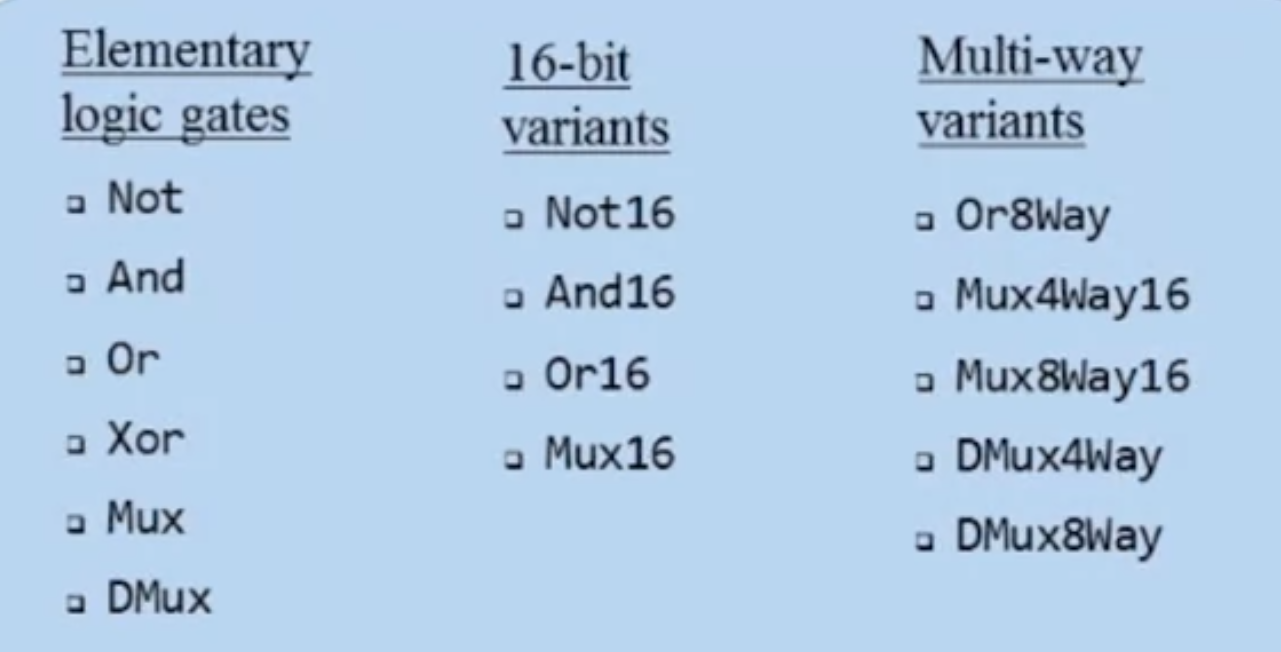
To construct a multi-bus version of a gate, imagine building the same one N times with no change!
eg. A Mux16 is simply 16 Mux (a=a[i], b=b[i], out=out[i]);
To do 4 way Mux, combine 2 stages of 2 way Muxes as such:
stage 1: two regular 2 way Muxes controlled by sel[0],
stage 2: one regular 2 way Mux controlled by sel[1].
Any 2^n order Mux can be constructed using 2 stages where stage 1 has two 2^(n-1) Muxes and the last stage has one 2 way Mux.
Addition:
Half adders have no memory of previous carry bit
sum = aXORb, carry=aANDb
Full adders have an input for previous carry
sum = aXORbXORc, carry = aXANDb + aXANDc (There has to be a better way to implement this in boolean logic).
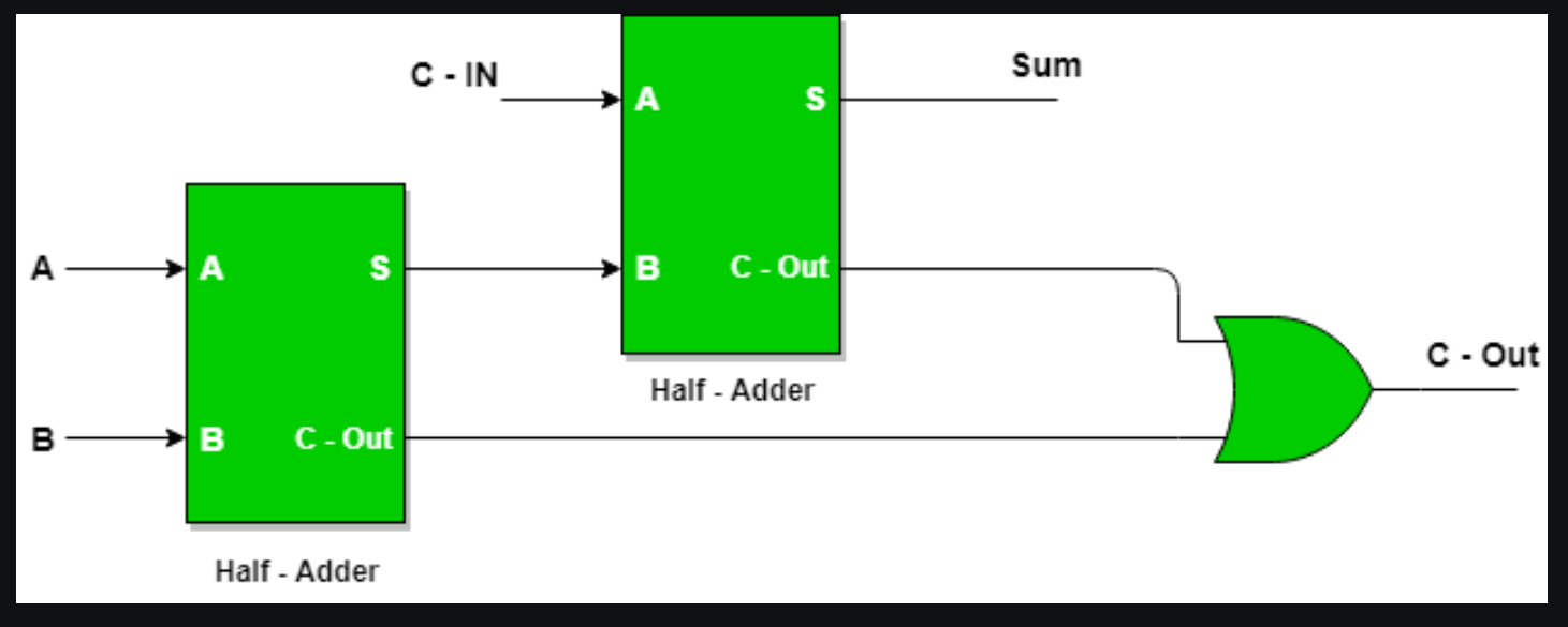
A full adder can be built from 2 half adders as such:
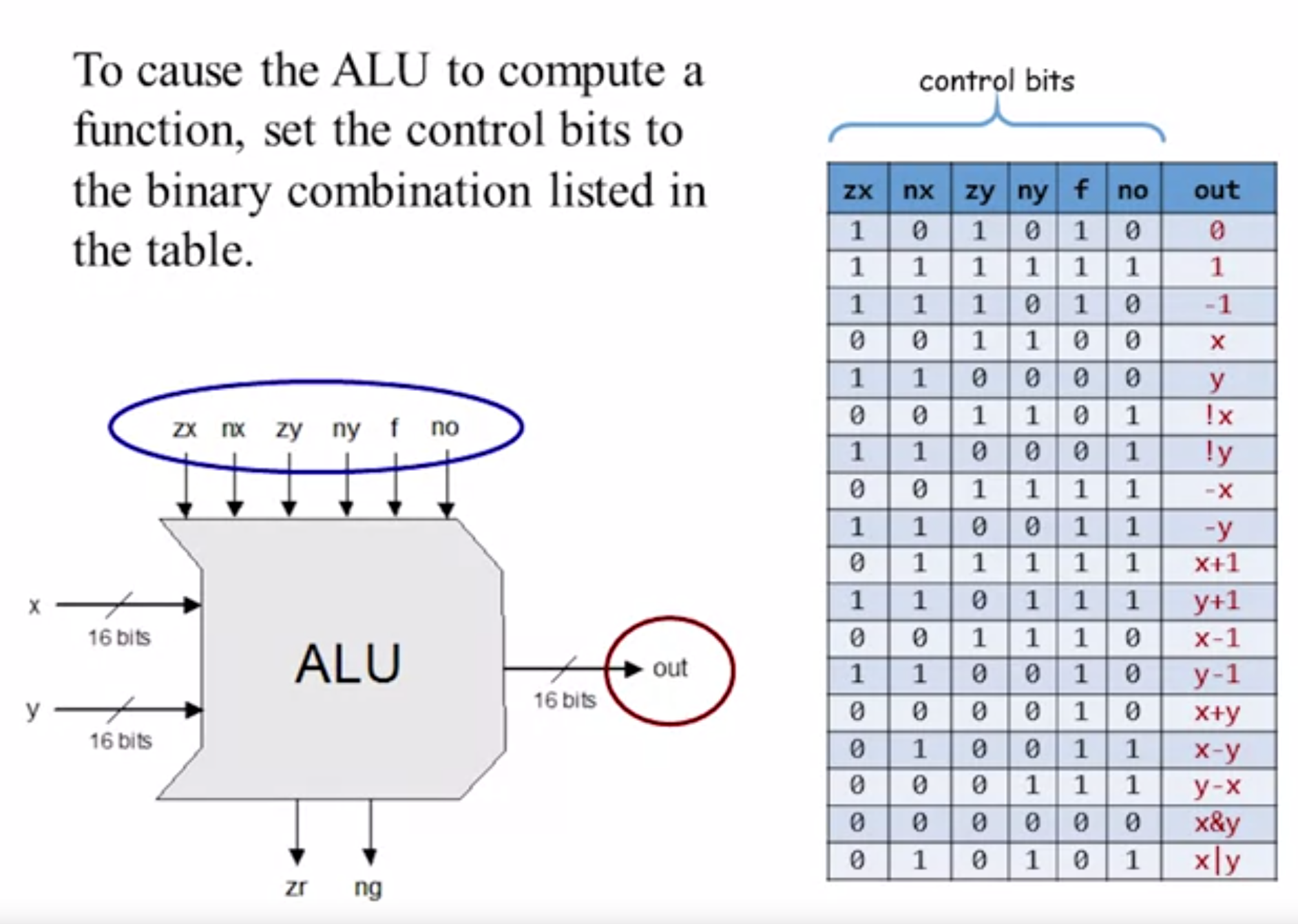
| Op | OPCODE |
|---|---|
| 0 | 0x2A |
| 1 | 0x3F |
| -1 | 0x3A |
| x | 0x0C |
| y | 0x30 |
| !x | 0x0D |
| !y | 0x31 |
| -x | 0x0F |
| -y | 0x33 |
| x+1 | 0x1F |
| y+1 | 0x37 |
| x-1 | 0x0E |
| y-1 | 0x32 |
| x+y | 0x02 |
| x-y | 0x13 |
| y-x | 0x07 |
| x&y | 0x00 |
| x | y |
Table 1. Available operations on the Hack ALU
min clock cycle = propagation delays + combinatoral delay
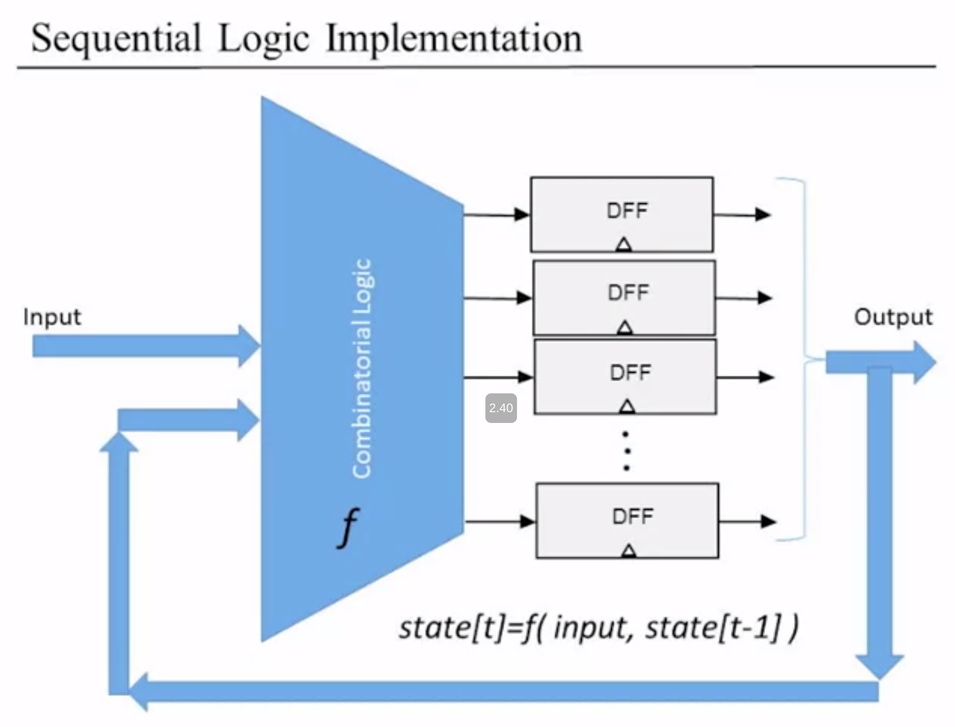
Sequential logic has the output out[t] depend on the previous output out[t-1]
We can use states to make the same hardware do different tasks. state[n] = function(state[n-1])
Circuits that can remember one bit of information during a transition. In a pipeline, no states are saved but rather passed onto the next combinatoral logic block in a chain to the output. In a finite state machine, the state at one instance is input to the combinatoral block that made it and contributes to the next state.
REGISTERS 4 inputs: clock, in, out, and load. If load[n-1], out[n]=in[n-1] else, out[n]=out[n-1]
In the von Neumann architecture, the memory registers connect to the ALU.
A sequence of n addressible registers pointed by an address input log(n) bits wide. Each register in the RAM has one word of data (16 bits in the Hack computer's case => 4 address bits). To read, set address to the location of the register and advance one clock cycle. Only one register is accessed at a single time.
To write, set address to location of register, set input to write value, then assert load (load=1). The write value is passed onto the register.
A program counter has 6 inputs: load, reset, increment, input, clock and address. When inc is asserted, out[n+1]=out[n]+1 after each clock cycle. When reset is asserted, out[n+1]=0.
Arithmetic operations: add, inc, ... Logical operations: and, or, ... Flow control operations: if x goto y, ...
Accessing memory locations is expensive. The smaller the memory going into the CPU, the faster access times we can get.
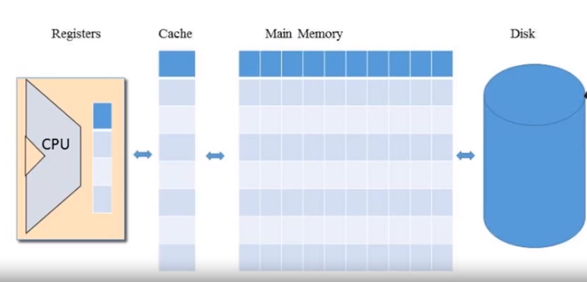 CPU <--> Registers >> Cache >> Main memory >> Disk
The CPU can access the registers very quickly. The registers can store data or point to memory addresss in another memory bank
store R1, @A; tells the computer to store the value of register R1 in a location of RAM given by the contents of register A.
Addressing Modes
- Register Add R1, R2; R2 = R2 + R1
- Direct Add R1, M[200]; M[200] is a memory unit in RAM, M[200] = M[200] + R1
- Indirect Add R1, @A; M[A] = M[A] + R1
- Immediate Add 714, R1; R1 = R1 + 714
Flow Control
Such as jump 102 which takes the program counter to the 102th instruction location every time the PC gets to this instruction. Or a conditional jump statement.
CPU Registers: D - data register A - address register M - register holding the value of one address in RAM specified by A.
Setting A automatically sets M as the value of M only depends on the location pointed to by A.
Syntax of A: @1242; sets the location to 1242 and the value of M to whatever is stored in RAM location 1242 This is how we load and store values from our memory.
To store the value 0x1000 in register 0x3FF, @0x3FF; sets the location and the value of M M=0x1000;
!! M isn't a copy of whatever value is stored in the RAM location so it could be closer to the CPU, it is the actual memory register itself !!
M=RAM[A]
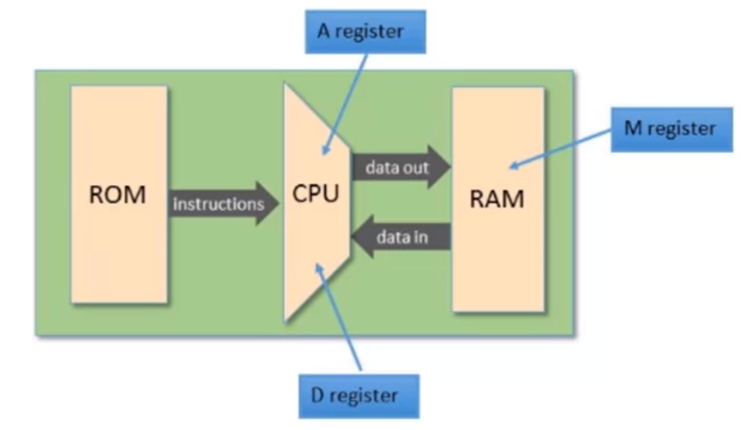
The Hack machine language is made out of 16-bit A or C instructions. (There is also a reset button used to start program execution.)
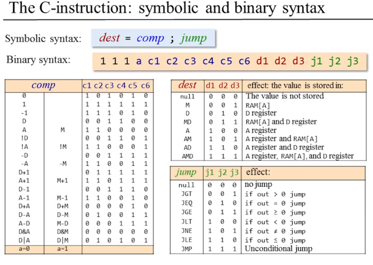
dest = comp; jump
jump and dest are optional instructions when executing this instruction, a computation is made after which some value is stored in a register or the program jumps to another instruction.
Comp can be any of the following instructions done on the A, D, and M registers:
| 0, 1, -1, D, A, M, | | !D, !A, !M, | | -D, -A, -M, | | D+1, A+1, M+1, D-1, A-1, M-1,| | D+A, D+M, D-A, D-M, | | A-D, M-D, | | D&A, D&M, | | D|A, D|M |
| |
There are 8 possible destinations:
- null - don't store computation in memory
- M
- D
- A
- AM - in both A and M
- AD
- MD
- AMD - in all registers
Jump conditions compare the output to zero and jump to the instruction given by the value of A register:
- null - don't jump
- JEQ - Jump (if) EQual
- JNE - Jump (if) Not Equal
- JGT - Jump (if) Greater Than
- JLT
- JGE - Jump (if) Greater than or Equal
- JLE
- JMP - Jump regardless
Some examples: // Set RAM[300] to the value of D -1 @300 // A instruction to set M to the location RAM[300] M = D-1 // Selected RAM location now loaded with value D-1
    // If D - 1 is zero, jump to execute instruction stored in ROM[56]
    @56     // A = 0x0038
    D - 1; JEQ      // Jump to instruction 0x0038 if D-1=0
Writing assembly can be done symbolically as shown above or using a binary syntax where we describe the instruction as a 16-bit code.
Binary Syntax: The MSB is our opcode: it says whether the instruction is A (0) or C(1). For A instructions, it is sufficient to simply state the memory location we want to address:
@100 // is equivalent to ... 0000000001100100
In the C instructions, the 14th and 15th bits are not used for anything and are just left as 1s. There are 3 bits to represent the 8 destination locations as well as 3 bits for the 8 possible jump instructions.
We need a screen and keyboard at the minimum. Their values are both stored in a dedicated sector of the RAM.
To display a 256x512 pixel screen (2^17), we'll need to assign a bit to each pixel. That means our screen memory map needs to be: $$ \frac{2^{17}\ bits}{2^4\ bits\ per\ word} = 8KB\ of\ memory $$
Our screen chip is simply an 8K RAM module that is a part of our bigger memory chip.
(Our system is 16 bits meaning all our registers only work on 16 bit values i.e. you can't just change one bit on the memory you'll have to change the entire word - R/W operations all work on words).
To set a pixel on/off we have to find what bit controls it by mapping from (pixel row, pixel col) to our 8KB memory location.
However, since the Screen memory is only a part of the bigger RAM that's been assigned to start at memory location 0x4000 (16K), we have to offset by 16K
Load the word location from the RAM to M using A, set the col % 16 th bit to 0 or 1 (perhaps by OR16-ing it with a mask...) and store back into M.
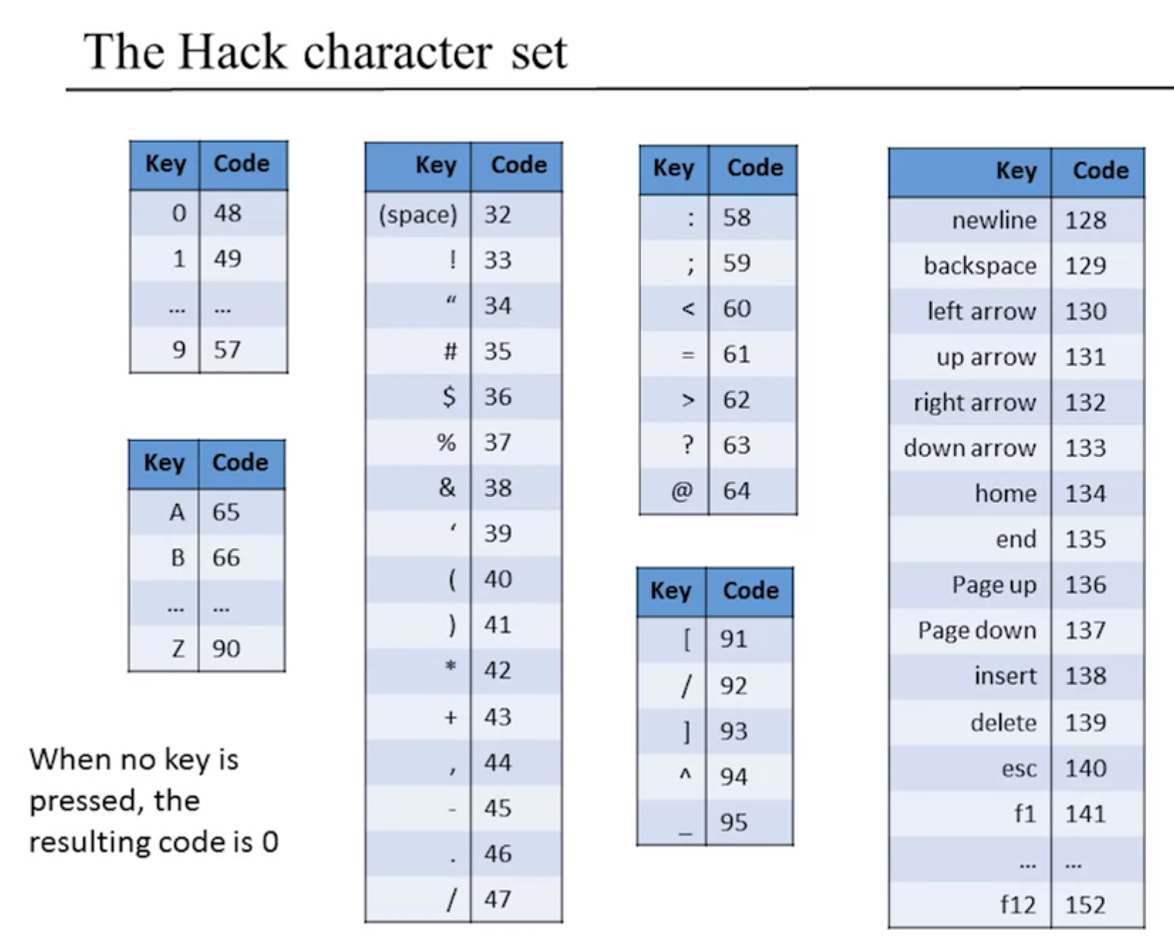
A keyboard only needs one word to store all possible states. Set to be RAM location 24,576. Only when the key is pressed, the register is set to the value of the character set that corresponds to that key. (eg. if A is pressed, code=65, register = 0x0041)
To check whether a key is pressed, we probe the contents of the Keyboard chip (register).
Load
    // set D = 10
    @10
    D=A

    // D = RAM[17]
    @17
    D=M
Store
    // RAM[1234] = D
    @1234
    M=D

    // RAM[1234] = 10
    @10
    D=A
    @1234
    M=D

    // RAM[5] = RAM[3]
    @3
    D=A
    @5
    M=D
    // Compute RAM[2] = RAM[1] + RAM[0]
    // dest = comp; jmp
    @0
    D=M  // D = RAM[0]
    @1
    D=D+M  // D+= RAM[1]
    @2
    M=D  // M = RAM[2] = RAM[0] + RAM[1]
Terminating a program properly: To stop the PC from going down in our memory and executing unwanted instructions, we can start a small loop after all our programs as such:
    //prog
   0 ...
   1 ...
   2 ...
   3 ...
   .
   .
   .
   47 @47
   48 0; JMP // jump to the memory location 47
Virtal registers: R0-15. Registers symbolically correspond to the first 16 addresses in the memory. Why?
    // To make RAM[5] = 14389
    // instead of doing the follg
    @14389
    D=A
    @5
    M=D

    // Do this
    @14389
    D=A
    @R5
    M=D
    // To make what we're doing less ambiguous
eg
    // R0 > 0 ? (R1=1):(R1=0)
    1 @R0
    2 D=M

    3 @9
    4 D; JGT // If D(=R0) > 0, jump to 9

    5 @R1  // If you reach here then R0 < 0
    6 M=0
    7 @11
    8 0; JMP  // Set R0 to zero; start inf loop

    9 @R1
    10 M=1

    11 @10
    12 0; JMP
Declare a meaningful label instead of a number to jump to so you understand what you're doing.
@LABEL is equivalent to @n
Put (LABEL) above the line of code you want to branch to in order to jump to that line.
    // R0 > 0  ? (R1=1):(R1=0)
    @R0
    D=M

    @POSITIVE_CASE
    D; JGT

    @R1
    M=0
    @END_PROG
    0; JMP

(POSITIVE_CASE)
    @R1
    M=1

(END)
    @END
    0; JMP
Variables: Use @var_name to assign a random memory location after register 15 that's not being used by the program to use for storing values. A branching symbol has a label declaration somewhere in the program while a variable doesn't.
QUICK TIP: Variable declaration
    // to set, say, n = 100
    @100
    D=A         // D=100
    @n          // set M to an unknown memory location n <=> RAM[x] to hold the variable n
    M=D         // n (= M = RAM[x]) = 100

    // 4 lines
    @value_for_var
    D=A
    @var
    M=D         // var=value_for_val

    // If the value you want to store in the variable is only 1, -1 or 0, we don't need to go through the data register to assign M

    @is_open
    M=0     // is_open=0
The operations 0, 1, -1, register + 1, register - 1, ... (all the comp instructions) can be executed on the M register directly without invoking the D register.
Always write pseudocode/flowcharts before making an asm! It also doesn't hurt to make a trace table!
    // Make an asm program to sum the numbers from 0 upto RAM[0] and store
    // their result in R1.
QUICK TIP: Making a for loop
    //  eg.
    n = 10;
    for (i=0; i<n; i++){
        arr[i] = -1;
    }
Assign the variables in the loop: arr, i, n (let the array start from memory location 100).
    // Pseudocode:
    arr = 100
    n = 10
    i = 0

    D=i-n
    D; JEQ to END
    // else
    RAM[arr+i] = -1
    i++
Using a pointer means assigning a variable to store a memory address.
    // Implementation

    // i=0
    @i
    M=0

    // n=10
    @10
    D=A
    @n
    M=D

    // arr=100
    @100
    D=A
    @arr
    M=D

(LOOP)
    @i
    D=M     // D=i
    @n
    D=D-M   // D=D-n=i-n
    @END
    D; JEQ

    // below only executes if loop is running:
    @arr
    D=M
    @i
    // watch this:
    A=D+M
    M=-1 // Here we set the next memory location depending on the value of
         // address plus an offset i. We pointed to the location we want and
         // changed the value of RAM there.
    @i
    M=M+1 // increment i by 1

    @LOOP
    0; JMP


(END)
    @END
    0; JMP
For convenience, the location 16,384 is assigned the variable SCREEN and 24,576 is KBD.
eg. Draw a filled rectangle at the upper corner of the screen, 16 pixels wide and RAM[0]=R0 pixels long.
    // Pseudocode
    // Remember the screen memory map
    // for (i=0; i<n; i++){
    // draw_16_black_pixels_beginning_from_row_i();
    // }

    //  addr = SCREEN;
    //  n = RAM[0];
    //  i = 0;

    //  LOOP:
    //      if i > n goto END
    //      else
    //          RAM[addr] = 0x1111 // = -1;
    //          addr += 32;
    //          i++;
    //          goto LOOP
    //  END:
    //      goto END
A single line of pixels is 32 registers wide, so to go to the next line, our address must increment by 32.
    // Implementation
    @R0
    D=M
    @n
    M=D // n=RAM[0]

    @i
    M=0 // i=0

    @SCREEN
    D=A  // We want the memory location itself not the contents!
    @addr  // addr = RAM[SCREEN]
    M=D

(LOOP) // i - n < 0
    @i
    D=M // D=i
    @n
    D=D-M // D=i-n
    @END
    D; JEQ

    @SCREEN
    M=-1  // RAM[SCREEN] = 0x1111

    @i
    M=M+1 // i++

    @32
    D=A  //  WE WANT THE VALUE 32 not the contents of register 32!
    @addr
    M=M+D  // addr += 32
    @LOOP
    0; JMP

(END)
    @END
    0; JMP
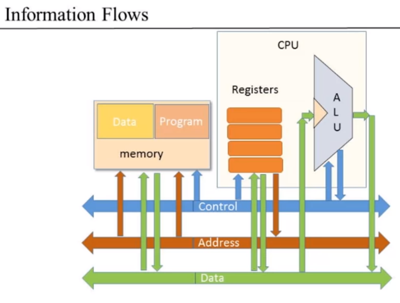
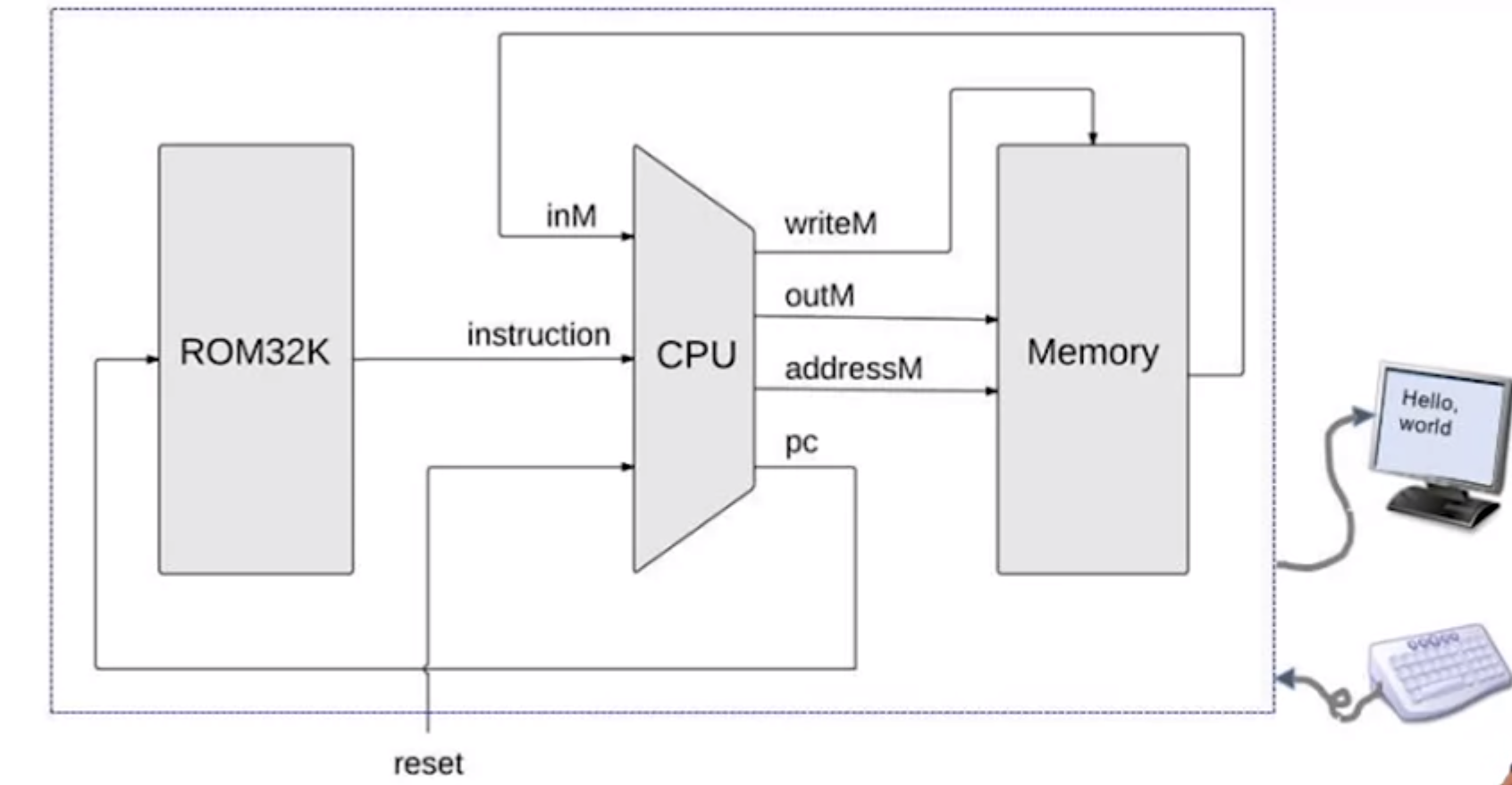
3 Buses: Control, Data, Address.
Loads information from the data bus and manipulates it using the control bits.
Load or store data and addresses.
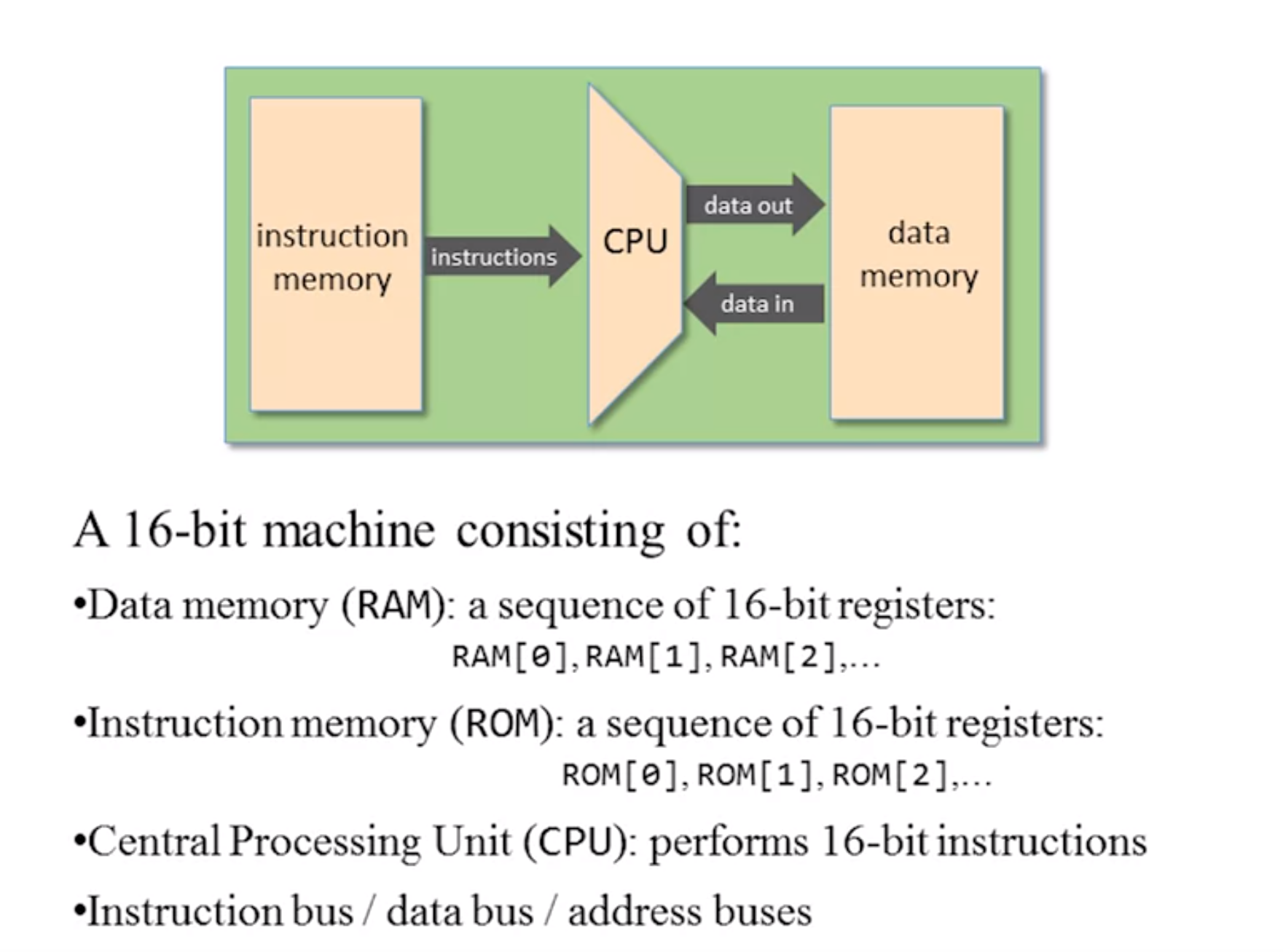
Divided into our data (RAM) and program (ROM). The data memory loads and stores data or addresses. The program memory stores all the program instructions. It needs to be fed by an address (the program counter) and has to be initially loaded with instruction data. It must then output into the control bus to control the flow of data and instructions to make the program execute.
All a CPU does at every cycle is fetch its next instruction from the program counter address in ROM, and execute the instruction.
When fetching, we put the location of the next instruction in our program counter. Takes control bits and data bits to output data (Read memory location PC in ROM) In branching, the PC gets loaded by some value next cycle, otherwise, the value of PC gets incremented by 1 in this clock cycle.
When executing, we take the opcode we fetched and load it to the CPU. We also need to access our registers and/or data memory as inputs to our ALU.
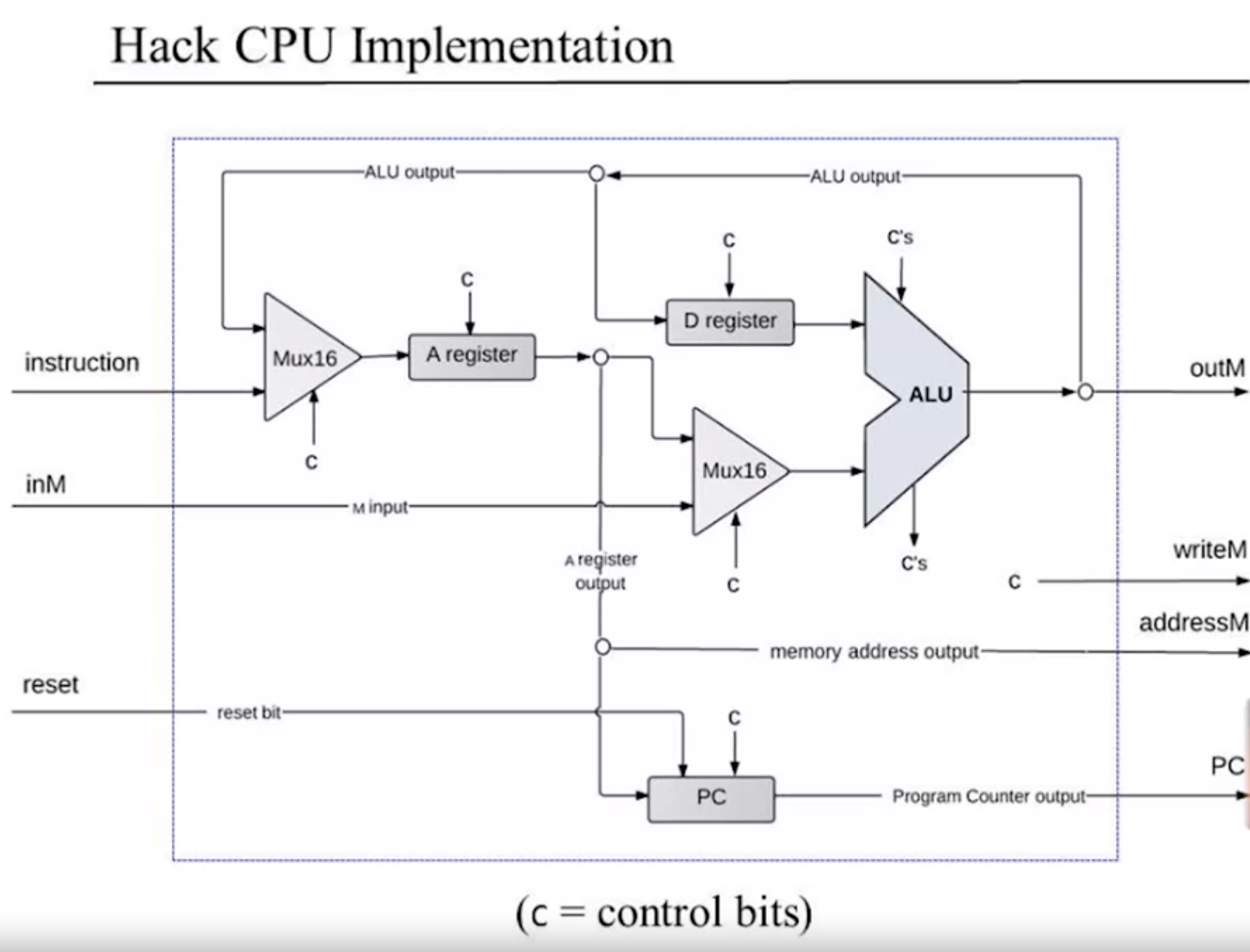
The CPU interface: Inputs
- Instruction 16-bits
- In_from_memory 16-bits
- reset 1-bit
Outputs
- Out_to_memory 16-bits
- Write_to_memory 1-bit
- Memory_address_output 16-bit
- Program counter 16-bit
Instruction Handling:
A-XX-C-CCCCCC-DDD-JJJ
The MSB is 1 for a C instruction and 0 for an A instruction. The instruction bits are decoded into 6 ALU control bits, 3 destination control bits and 3 jump bits.
Input --> Instruction Memory (ROM) => CPU <=> Data Memory (RAM) --> Output
Translate asm into machine code. Multi-pass assemblers pass through the code once while taking note of all labels so jump instructions can be interpreted on the second run. Single-pass assemblers only go through the code once.
Building a cross-compiler to take in assembly commands and output machine code:
-
read the asm line by line
load R1, 18 -
break each line into different asm fields ingore whitespace
break into load, R1, 18 find opcode for load,
find opcode for R1,
translate 18 into binary,
fill remaining bits in instruction
Symbols: labels and variables replace labels with the line of asm at which they are declared.
replace variables with the binary representation of the value they hold. Keep a running key-value pair corresponding to each symbol and its value. Variables are automatically stored in the next unused register after register 15. This means our first variable declared goes into the 16th register, our second goes into the 17th register and so on.
In a multi-pass assembler, go through the code once just keeping track of these associations on a table before going through the code again with them replaced.
Labels! These can be forward referenced, which means the location it points to hasn't been reached yet. To do this in a single-pass, ...?
- look up the binary code associated with each field (use dicts?)
- combine different fields with their associated code to make a 16-bit instruction
- output line and go to next line in asm
###Language specification
-
A instructions I[15] set to 0
@value; value can be a non-negative decimal or a symbol for a variable
eg. @21 -> 0000-0000-0001-0101 // (dashes put just for clarity)
-
C instructions
dest = comp; jump
Binary syntax: 111-a-c1c2c3c4c5c6-d1d2d3-j1j2j3
Refer to the hack language specification to see what a specific command like JEQ corresponds to in machine code (it's 010 for j1j2j3)
Symbols: pre-defined symbols
[R0, R15] -> [0, 15]
SCREEN -> 16384
KBD -> 24576
SP -> 0
LCL -> 1
ARG -> 2
THIS -> 3
THAT -> 4
Comments: If you get to a '//' section in a line, ignore (better yet, sanitize the strings by splitting by '//' and only take the first part of the output) Remove all white space by splitting by ' ')
steps to take to parse asm:
- remove all white space
- remove all symbols
Translating A instructions Change number to binary representation in 15 bits, if a variable is used, assign that to (i + 16) where i is the index of the var in a list of all variables.
Target expression: 0-BINARY_REP_IN_15_BITS
Translating C instructions Refer, again, to the language specification.
eg. MD=D+1 // dest = cmp; jmp // maybe split by ';', then '='
Always split into three fields: dest, cmp, jmp
If jmp field isn't filled, j1j2j3=000
Target expression: 111-a-c1c2c3c4c5c6-d1d2d3-j1j2j3 for MD=D+1 Target expression: 111-0-011111-011-000
think of a as a pre-comp bit and form your binary table of comp with a.
- Variable Symbols
if a variable is used, assign that to (i + 16) where i is the index of the var in a list of all variables.
pseudo-code:
func    read_line(line)
    if line[0] == '@':
       var_or_num = line[1:]
       if var_or_num.is_number():  # check if its a number or string
            opcode = '0' + binary_15(int(var_or_num))
        else:
            if var_or_num not in list_of_vars:
                list_of_vars.append(var_or_num)
            else:
                opcode = '0' + binary_15(16 + index(var_or_num))
    # ... code for C instruction here
    return opcode
- Label Symbols
Declared by pseudo-command (XXX).
Now, whenever, the symbol xxx is encountered in the program, jump to the line
right after that pseudo-command declaration.
(In code, do a pass of the code only making key-value associations between each label and its corresponding address in decimal, then removing that line)
When making a multi-pass assembler, scan the entire program keeping a dict.
Pseudo-code:
    rom_instr = []
    for line in lines:
        line = remove_whitespace(line)
        if is_instr(line):
            line.append(rom_instr)
        else:
            if line[0] == '(':
            label = line[1:-2]
            symbol_lkp.key(label) = len(rom_instr) + 1
            # assign next instruction address to value of label
- Pre-defined Symbols Just replace with their decimal number from a lookup
Read a file line by line. Get fields. Break into tokens.
Lookup table for C instruction fields
like this D_lkp = {"D": "000"}
