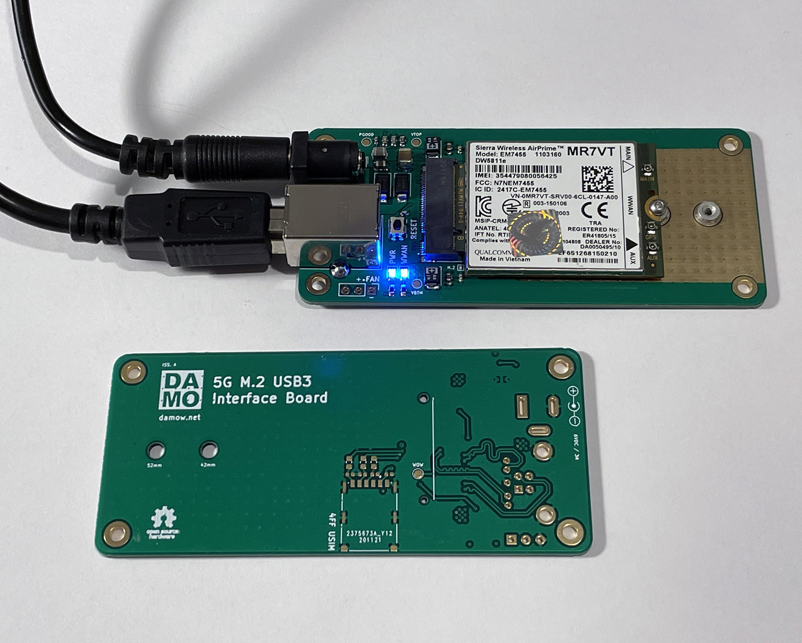
I’ve been experimenting with 5G cellular modules recently, and found that many of the M.2 break-out boards that run on just USB power (mostly designed for 4G modules) can’t supply the required current at the peaks during transmission. I decided to design my own in KiCad with dual-power input, Nano-SIM slot, and USB 3 to support the required data rates for 5G.
I'm using mine with a Quectel RM500Q-GL 5G module that I've previously blogged about. The design very much obeys the appnote recommendations for the RM500Q-GL module so use with that one especially should work fine.
- Compact size, 90mm x 40mm board size; with 82mm x 32mm spaced M2.5 mounting holes
- USB 3.0 SuperSpeed for high 5G data rates
- Dual-power input.
- USB 3.0 B (not recommended for heavy data use, but fine for lower-end modules)
- 5-9V DC 5.5mm barrel jack (centre-positive)
- Fits both 52mm and 42mm M.2 B-Key modules
- Single 4FF Nano-SIM USIM slot
- Module reset button
- Module WWAN LED
- Power LED
- 5V 3-pin fan header
4 layers. Standard FR4. ENIG recommended for easier soldering of the fine-pitch parts (M.2 connector & TPS82130SILR DC-DC converter)
BOM can be found in the bom/ directory. Currency is GBP. Total build cost (excluding non-special caps & resistors) is ~£15 in 10qty.
Open an issue or drop me an email - me@ my blog domain.
