Design of a 1.2MS/s Charge-Redistribution Non-Binary SAR-ADC utilizing the SKY130 Open-Source Technology
Author: Manuel Moser, 2023, Johannes Kepler University (JKU) Linz, Austria, Institute for Integrated Circuits (IIC).
This SAR-ADC has been designed in the context of a Master's thesis, it is published on the JKU ePUB repository.
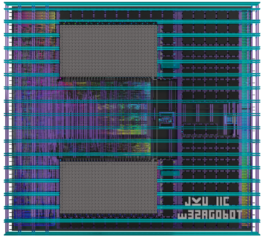
 Figure 1: 3D render of the SAR-ADC layout made with Blender and gdsiistl.
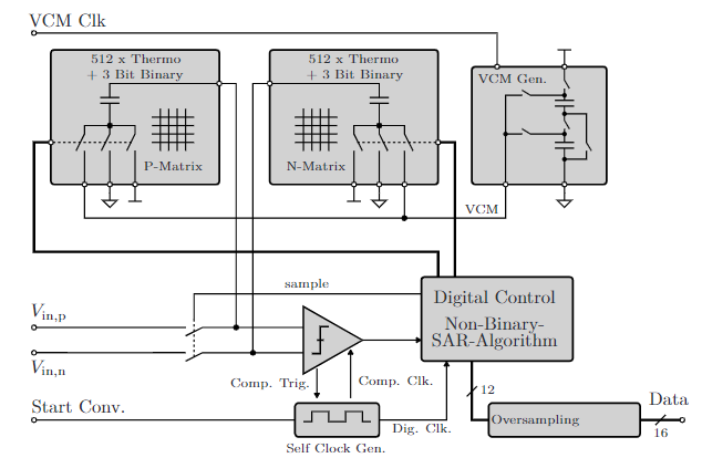
The proposed design is a versatile non-binary, asynchronous (= self clocked) 12 bit SAR-ADC (successive approximation register analog-to-digital converter), using a segmented 12 bit capacitive DAC with 9 bit thermometer-coded capacitor array and 3 bit binary capacitor cells. The SAR-ADC Layout has previously been added to the IIC Mixed-Signal Circuits Submission for the Open MPW-8 Shuttle.

Figure 2: The block diagram of the proposed 12-bit SAR-ADC. Image obtained and adapted from [1].
- Differential analog inputs.
- ADC physical resolution of 12 bit, up to 16 bit with oversampling.
- Sample rate configurable in a broad range from 28S/s (low-power biosensor applications) up to 1.2MS/s.
- Non-binary SAR weights for error correction capability.
- Oversampling FIR boxcar filter with 1/4/16/64/256 samples to increase the resolution.
- Averaging of 4 least significant SAR weights with 1/3/7/15/31 samples to reduce the impact of comparator noise.
- Clock generator with a configurable frequency. The clock generator layout has been hardened with
OpenLaneusing a gate level description of the clock loop. The delay elements in the loop use a custom high-delay standard cellsky130_mm_sc__hd_dlyPoly5nswhich fits into thesky130_fd_sc__hd_standard cell grid. - Integrated switched capacitor voltage generator for the common mode reference voltage.
- 12 bit capacitor DAC:
- Unit capacitor with
$C^{1}$ =0.447 fF. - 3 bit binary-coded cells with 1x1, 1x2 and 1x4 unit capacitors
$C^{1}$ +$C^{2}$ +$C^{4}$ for LSB bits. - 9 bit thermometer-coded cells with 1x8 unit capacitors
$C^{8}_{1..511}$ =3.58 fF. - The total capacitance per DAC matric is 1.83 pF.
- Unit capacitor with
- The thermometer-code row/column decoder can be switched from a sequential to a symmetrical mode to decrease the integral nonlinearity error.
- Total area of
$442 \mu m \cdot 402\mu m = 178.000 \mu m^2$ , the area decreases to$124.000 \mu m^2$ if the$V_\mathrm{CM}$ voltage generator is not included. - 100% open source, licensed with Apache 2.0
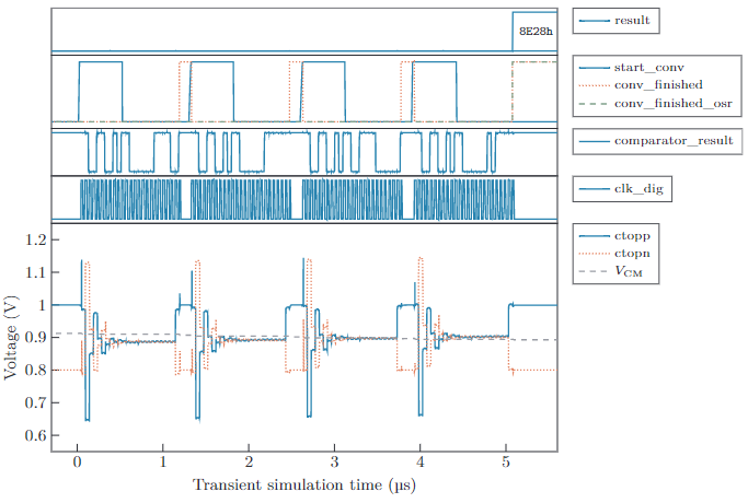
Characterization of the ADC has been done through post-layout simulation with parasitic C extraction. For the typical setting, the SAR-ADC has been configured to use 3 samples per LSB averaging, 4 samples oversampling, and a symmetric thermometer-code sequence. The clock generator has been set to use the lowest delay configurations (00001), as a result, the ADC is sampling at 824 kS/s with a Nyquist bandwidth of 103 kHz. The waveforms obtained in the simulation can be seen in Fig. 3, and the results are summarized in Table 1.

Figure 3: The plots show the simulation result of the post-layout simulation at 3 samples per average, oversampling factor 4, and 824 kS/s sample rate.
Table 1: Summary of the SAR-ADC characteristics obtained from simulation.
| Parameter | Min | Typ | Max |
|---|---|---|---|
|
|
- | - | |
| Area (µm²) | - | ||
| DAC resolution (bit) | - | - | |
| Result (bit) | - | ||
| Oversampling factor | |||
| LSB Averaging (samples) | |||
| Sample rate (kS/s) | |||
| Nyquist Bandwidth (kHz) | |||
| Average PD (µW) | - |
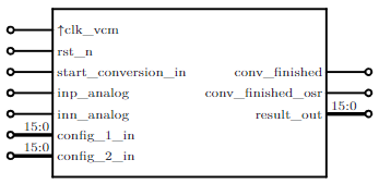
The configuration bytes config_1_in and config_2_in are used to activate the sequential/symmetrical row/column decoder modes and to configure the delays in the self-clocked loop. The configuration port mapping is described in doc/interface.md. rst_n will reset the circuit active-low. After reset de-assertion the circuit waits for the trigger signal start_conversion_in, an edge-detection-circuit ensures that only one conversion is triggered if the start signal stays high. A single conversion is done when conversion_finished_out changes to HIGH, additionally, conversion_finished_osr_out signalizes a finished OSR sequence and an update of the result at the output. Input signal clk_vcm is the clock signal for the switched-capacitor voltage generator, it is designed for a low frequency of 32.768 kHz.

Figure 4: Block diagram of the SAR-ADC
//Top module ADC Control
module adc_top(
   `ifdef USE_POWER_PINS
      inout VDD,	// User area 1.8V supply
      inout VSS,	// User area ground
   `endif
   input wire clk_vcm,        // 32.768Hz VCM generation clock
   input wire rst_n,          // reset
   input wire inp_analog,     // P differential input
   input wire inn_analog,     // N differential input
   input wire start_conversion_in,
   input wire [15:0] config_1_in,
   input wire [15:0] config_2_in,
   output wire [15:0] result_out,       // format: {12 bit, 4 bit OSR extension}
   output wire conversion_finished_out,
   output wire conversion_finished_osr_out
);[1] S. Schmickl, T. Faseth and H. Pretl, "An Untrimmed 14-bit Non-Binary SAR-ADC Using 0.37 fF-Capacitors in 180 nm for 1.1 µW at 4 kS/s," 2020 27th IEEE International Conference on Electronics, Circuits and Systems (ICECS), Glasgow, UK, 2020, pp. 1-4, doi: 10.1109/ICECS49266.2020.9294971.