中文 | English
FT232H、FT2232H、FT600 、 FT601 等芯片的 sync-245-fifo 模式的控制器,实现 FPGA 与 Host-PC 的高速通信。
sync-245-fifo 模式 (简称 245fifo 模式)是 FTDI 公司的 USB 系列芯片的最高速传输模式。本库将 245fifo 控制器封装成 Verilog 模块,留出精简的流式收发接口 ,供 Verilog 开发者调用。
另外,本库提供配套的:
- FPGA 示例工程
- 驱动安装教程
- Python 软件库安装教程
- 几个 Python 程序用于测试
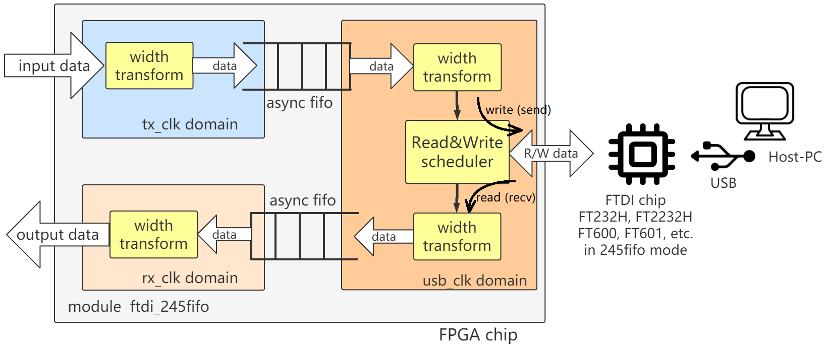
图1是该模块的结构框图。
 |
|---|
| 图1:ftdi_245fifo.sv 模块的结构框图 |
- 收发调度:FTDI USB 芯片与 FPGA 之间的接口是半双工的,该模块调度收发分时复用,实现 收发接口互相独立 。
- 跨时钟域:FTDI USB 芯片有自己的时钟。该模块用异步 FIFO 实现时钟域转换,使得收发接口可使用 自定义时钟 。
- 位宽变换:FTDI USB 芯片数据位宽是固定的,但本模块实现了位宽变换。收发接口的 位宽可自定义 。
以下是用本库测出来的 USB 上行(FPGA发,Host-PC收)的通信速率。
| 芯片型号 | FT232H 或 FT2232H | FT600 | FT601 |
|---|---|---|---|
| USB模式 | USB2.0 HS | USB3.0 SS | USB3.0 SS |
| 理论速率 | 60MBps | 200MBps | 400MBps |
| 实测速率 | 42MBps | 120MBps | 未测 |
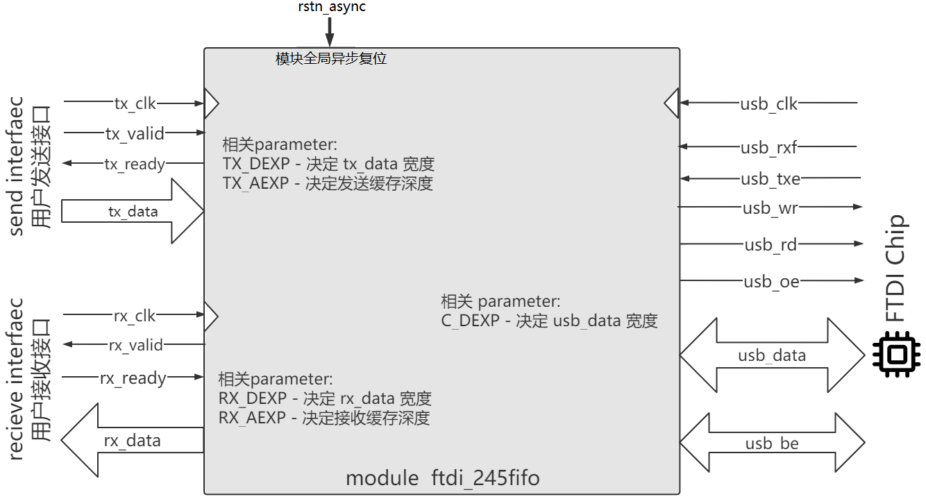
本库的设计代码是 RTL 目录中的 ftdi_245fifo.sv,供 FPGA 开发者调用来开发自己的 USB 通信业务,它的接口和参数如图2。
 |
|---|
| 图2:ftdi_245fifo.sv 的接口 |
要调用本模块,首先要根据实际情况确定各个参数 (Verilog parameter) 的值,如下表:
| parameter | 说明 |
|---|---|
| TX_DEXP | 决定了用户发送接口的数据宽度(即tx_data的宽度):0对应8bit宽,1对应16bit宽,2对应32bit宽,3对应64bit宽,以此类推。可以根据实际需要任意设置,不受所选的 USB 芯片型号限制。 |
| TX_AEXP | 决定了用户发送缓存的深度,深度=2^TX_AEXP。默认为10(即默认深度为1024),如果 FPGA BRAM 较大,该项可以设得更大,来提高突发性能。 |
| RX_DEXP | 决定了用户接收接口的数据宽度(即rx_data的宽度):0对应8bit宽,1对应16bit宽,2对应32bit宽,3对应64bit宽,以此类推。可以根据实际需要任意设置,不受所选的 USB 芯片型号限制。 |
| RX_AEXP | 决定了用户接收缓存的深度,深度=2^RX_AEXP。默认为10(即默认深度为1024),如果 FPGA BRAM 较大,该项可以设得更大,来提高突发性能。 |
| C_DEXP | 决定了USB数据信号(即usb_data)的宽度:0对应8bit宽,1对应16bit宽,2对应32bit宽,3对应64bit宽。应该根据所选的 USB 芯片型号而设置:FT232H设为0,FT600设为1,FT601设为2。 |
rstn_async 是模块的全局异步复位信号,0代表复位,1代表释放复位。在使用中,该信号可以直接设为 1'b1 ;或者连接到工程的复位信号上。
usb_rxf, usb_txe, usb_oe, usb_rd, usb_wr, usb_data, usb_be 这些信号应约束到 FPGA 的引脚上,连接到对应的 FTDI USB 芯片的引脚上。注意以下几点:
- FTDI USB 芯片工作在 245fifo 模式时,引脚名称见芯片 Datasheet(以 FT232H 为例,见 FT232H DataSheet 第9页)。
usb_be信号是字节独热码,仅 FT600 和 FT601 芯片有这个信号。对于 FT232H 和 FT2232H ,请忽略它。- 这些引脚的时序由模块维护,不需要你关注。如果你感兴趣,可以运行模块RTL仿真 。
本模块内置一个发送缓存,开发者需要提供一个 tx_clk 时钟,并在该时钟域下操作 tx_valid, tx_ready, tx_data 这三个信号,来把数据从 FPGA 发送到发送缓存,(Host-PC上启动接收程序时,发送缓存中的数据会自动发给PC)。注意以下几点:
tx_clk的频率不限,tx_valid,tx_ready,tx_data信号应该在tx_clk的上升沿更新或捕获。tx_valid=1时,说明用户想发送一个数据到模块内部的发送缓存。同时,tx_data应产生有效数据。tx_ready=1时,说明模块已经准备好接收发送数据。tx_ready=0时,发送缓存暂时满,不能接收更多数据。tx_valid与tx_ready是一对握手信号。二者同时为 1 时,tx_data写入缓存成功。
以如下波形图举例,在这个波形图中,用户接口发送了3个数据:D1, D2, D3 。其中:
-
第 1, 2 周期,用户令
tx_valid=0,因此暂时空闲没发数据。 -
第 3 周期,用户要发 D1,因此令
tx_valid=1,本周期tx_ready=1,说明 D1 即刻发送成功。 -
第 4, 5, 6, 7 周期,用户要发 D2,因此令
tx_valid=1,但第 4, 5, 6 周期tx_ready=0导致发送暂时失败,直到第 7 周期tx_ready=1时,才发送成功。 -
第 8, 9 周期,用户令
tx_valid=0,因此暂时空闲没发数据。 -
第 10 周期,用户要发 D3,因此令
tx_valid=1,本周期tx_ready=1,说明 D3 即刻发送成功。cycle 1 2 3 4 5 6 7 8 9 10 11 _ __ __ __ __ __ __ __ __ __ __ __ clk \__/ \__/ \__/ \__/ \__/ \__/ \__/ \__/ \__/ \__/ \__/ \ _____________________________ _____ tx_valid ___________/ \___________/ \________ _________________ ________________________________ tx_ready \_________________/ _____ _______________________ _____ tx_data XXXXXXXXXXXX__D1_X___________D2__________XXXXXXXXXXXXX__D3_XXXXXXXXX
本模块内置一个接收缓存,开发者需要提供一个 rx_clk 时钟,并在该时钟域下操作 rx_valid, rx_ready, rx_data 这三个信号,来把来自 Host-PC 的暂存在接收缓存内的数据拿出来。它与用户发送接口时序相同,但方向相反。注意以下几点:
rx_clk的频率不限(当然,可以和tx_clk接在同一个时钟上),rx_valid,rx_ready,rx_data信号应该在rx_clk的上升沿更新或捕获。rx_valid=1时,说明模块想发送一个数据给用户。同时,rx_data上出现有效数据。而rx_valid=0时,接收缓存空,不能拿出更多数据。rx_ready=1时,说明用户已经准备好拿出一个数据。rx_valid与rx_ready是一对握手信号。二者同时为 1 时,rx_data才成功从接收缓存中取出。
用户接收接口的时序类似用户发送接口(唯一的区别是方向相反),因此这里不再举例说明其波形图。
如果你好奇 ftdi_245fifo.sv 模块的设计细节,或者想了解 FTDI USB 芯片的 245fifo 模式的操作时序,可以运行仿真。
仿真相关的文件都在 SIM 文件夹中,其中:
- tb_ftdi_245fifo.sv 是针对 ftdi_245fifo.sv 的 testbench,它模拟了一个简单的 FT232H 的行为,并与 ftdi_245fifo.sv 互相交换数据。
- tb_ftdi_245fifo_run_iverilog.bat 是运行 iverilog 仿真的命令脚本。
使用 iverilog 进行仿真前,需要安装 iverilog ,见:iverilog_usage
然后双击 tb_ftdi_245fifo_run_iverilog.bat 运行仿真,然后可以打开生成的 dump.vcd 文件查看波形。
FT232H 是 USB2.0 High Speed 通信芯片,理论速率为 60MBps ,本例实现 FPGA 通过 FT232H 与 Host-PC 进行通信。
注:本例也适用于 FT2232H (具体操作时需要你自己变通变通),因为 FT2232H 与 FT232H 高度相似, FT2232H 的 channel A 可配置成与 FT232H 完全相同的 245fifo 接口 。
请按照 FTD2XX_guide.md 的指示在 Host-PC (Windows系统) 上安装 FTD2XX 驱动和 Python FTD2XX 库。
请使用以下源文件建立 FPGA 工程:
- RTL 文件夹里的 fpga_top_example_ft232h.sv :作为工程的顶层。
- RTL 文件夹里的 ftdi_245fifo.sv 、 stream_async_fifo.sv 、 stream_wtrans.sv :它们会被顶层调用。
然后,请在 FPGA 工程中进行引脚约束,具体而言,你需要查看电路板的原理图(或开发板配套资料),了解 FT232H 的各引脚被连接到了 FPGA 的哪些引脚号上;然后,把 FPGA 工程的顶层(也就是 fpga_top_example_ft232h.sv)的信号分配到对应的 FPGA 引脚号上,使得这些信号与 FT232H 的引脚对应起来。对应关系见下表(该表简化自 FT232H DataSheet 第9页):
| FT232H引脚号 | FT232H引脚名 | FT232H引脚名 (245fifo 模式下) | 应约束到顶层的信号名 |
|---|---|---|---|
| 13 | ADBUS0 | D0 | usb_data[0] |
| 14 | ADBUS1 | D1 | usb_data[1] |
| 15 | ADBUS2 | D2 | usb_data[2] |
| 16 | ADBUS3 | D3 | usb_data[3] |
| 17 | ADBUS4 | D4 | usb_data[4] |
| 18 | ADBUS5 | D5 | usb_data[5] |
| 19 | ADBUS6 | D6 | usb_data[6] |
| 20 | ADBUS7 | D7 | usb_data[7] |
| 21 | ACBUS0 | RXF# | usb_rxf |
| 25 | ACBUS1 | TXE# | usb_txe |
| 26 | ACBUS2 | RD# | usb_rd |
| 27 | ACBUS3 | WR# | usb_wr |
| 28 | ACBUS4 | SIWU# | usb_siwu * (=1) |
| 29 | ACBUS5 | CLKOUT | usb_clk |
| 30 | ACBUS6 | OE# | usb_oe |
| 31 | ACBUS7 | PWRSAV# | usb_pwrsav * (=1) |
| 34 | RESET# | RESET# | usb_resetn * (=1) |
*注:上表中 SIWU# 、 PWRSAV# 和 RESET# 实际上是永远被拉为高电平的(你也可以看到在 fpga_top_example_ft232h.sv 中它们被 assign 为 1),因此有些板子的设计直接用电阻把它们拉到高电平上,而没有连接到 FPGA ,对于这种情况,就不用在 FPGA 约束它们的引脚,并直接在 fpga_top_example_ft232h.sv 中注释掉与它们相关的语句即可。
注:对于 FT2232H ,请以 FT2232H DataSheet 第9页为准。
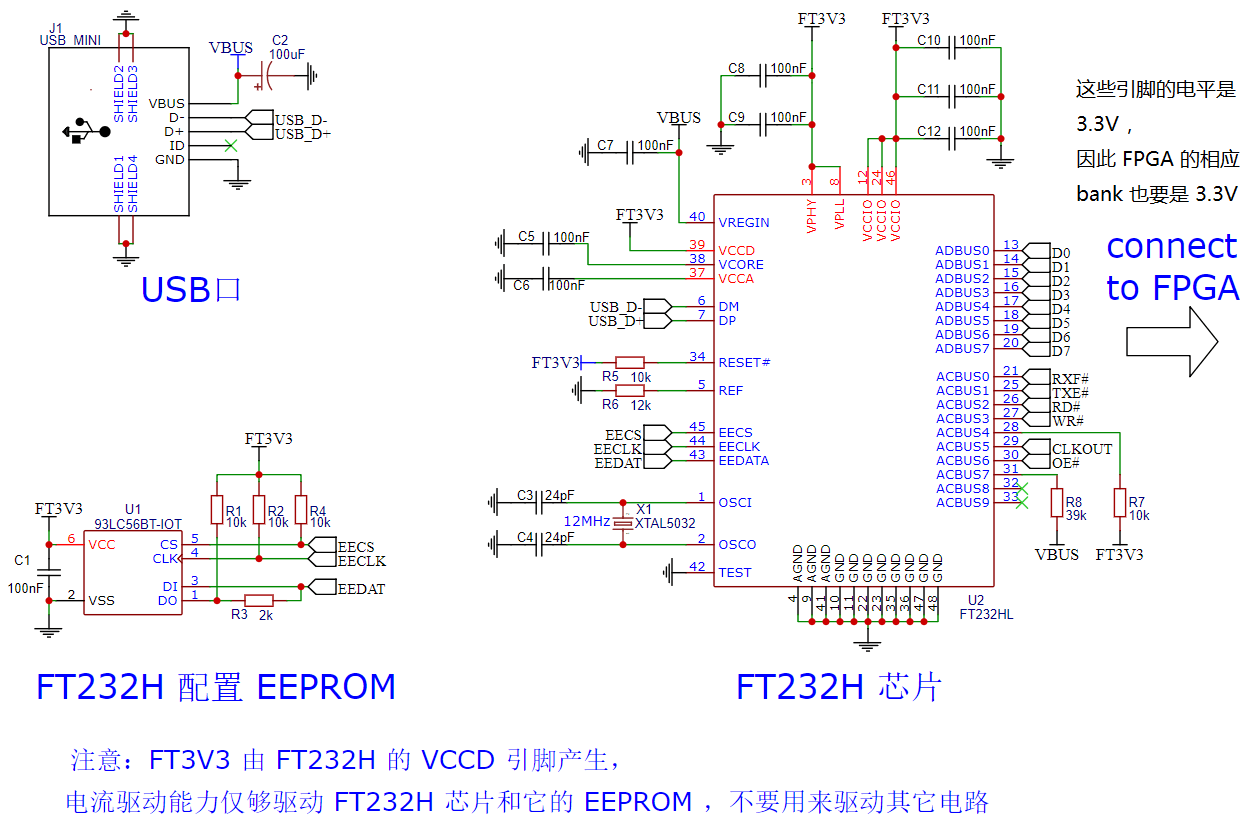
如果你要自己画 FT232H 的 PCB,可参考图3 。
 |
|---|
| 图3:FT232H USB 接口电路的参考原理图设计 |
在 FPGA 工程中,另外注意以下几点:
usb_clk频率为 60MHz 。你可以把usb_clk约束为 60MHz,来指导时序分析。实际上,即使不加该约束也不影响正常运行。- fpga_top_example_ft232h.sv 中的主时钟
clk要连在 FPGA 板的晶振上,频率不限,比如 24MHz, 50MHz, 100MHz 均可。 - led 引脚连一颗 LED 灯(不是必须的),它平常保持 1,当发现接收到的数据不是递增的时,会变成 0 并保持一秒。
- 请关注本例 fpga_top_example_ft232h.sv 中 ftdi_245fifo 模块的参数配置:
C_DEXP被设为 0,这是因为 FT232H 的数据线是 8bit 的。TX_DEXP被设为 3,因此用户发送接口的tx_data信号的宽度是 64bit (这只是本例的取值,你可以根据你的项目需要来修改)。RX_DEXP参数被设为 0,因此用户接收接口的rx_data信号的宽度是 8bit (这只是本例的取值,你可以根据你的项目需要来修改)。
然后你就可以编译工程,步骤略。
针对每颗 FT232H 芯片,需要在初次使用时烧录为 245fifo 模式。每颗 FT232H 芯片只需要烧录一次,因为 FT232H 外围会有个 EEPROM 芯片用来永久保存配置,之后每次使用都不需要再烧录(除非你又烧录了其它模式)。
首先进入 FT_Prog下载页面 下载并安装 FT_Prog 软件。然后进行以下步骤:
- 在电脑上插入你需要烧录的 FT232H 的 USB 接口,并拔出所有其它 FTDI USB 芯片设备(包括拔出所有的 FPGA 下载器,因为很多 FPGA 下载器,例如 Xilinx Digilent 下载器是 FT2232H 芯片实现的,如果万一覆盖了下载器内部的程序,你的下载器就废了)。
- 打开 FT_Prog 软件。
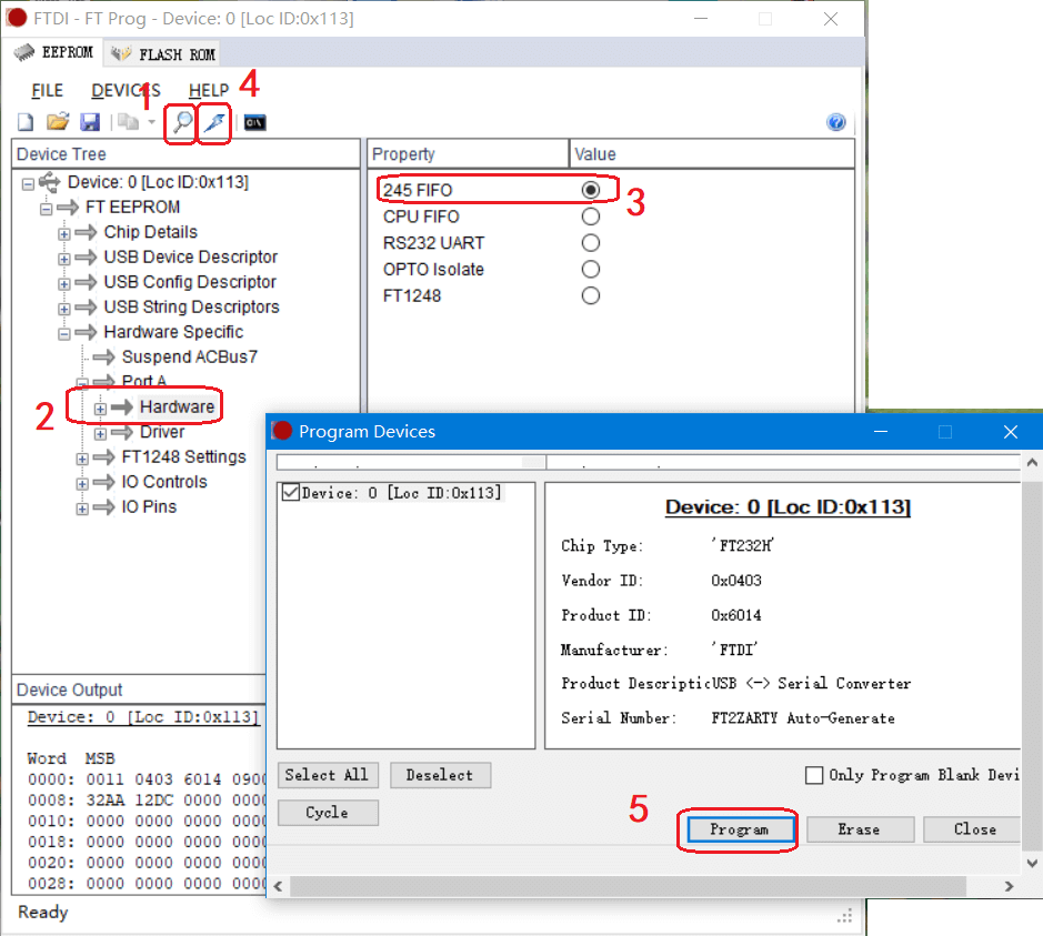
- 如图4,点击 Scan and Parse (图标为小放大镜) ,扫描出插在该电脑的所有 FTDI 芯片,找到 FT232H 对应的芯片。
- 在 FT232H 下方的属性树中逐级展开,找到并点击 Hardware 。
- 在右侧选择 245 FIFO 模式。
- 点击上方工具栏中的 Program (图标为小闪电)。
- 弹出确认窗口,点击 Program。烧录到 FT232H 。
- 烧录后,需要重新拔插 FT232H 的 USB 接口,该配置才能生效。
 |
|---|
| 图4:烧录 FT232H 芯片,配置为 245fifo 模式。 |
我在 python_ft232h 文件夹中提供了以下几个 Python 程序,它们会通过 FT232H 与 FPGA 进行通信。运行这些程序之前,请确保 FT232H 已经按照步骤3被烧录为 245fifo 模式,且 FPGA 中下载了步骤2中建立的工程。
| 文件名 | 功能 |
|---|---|
| USB_FT232H.py | 定义了 USB_FT232H_sync245mode 类,实现了 构造函数, close, send, recv 方法,它会被以下文件调用。 |
| usb_rx.py | 简单地试图接收 32 个字节(FPGA 发送,Host-PC 接收) |
| usb_tx.py | 简单地发送 16 个字节(FPGA 接收,Host-PC 发送) |
| usb_rx_rate.py | Host-PC 不断接收大量数据,并统计通信速率 |
| usb_rx_tx_validation.py | 同时进行收发正确性验证,它会不间断地发送和接收。因为配套的 FPGA 程序会发送的是递增数据,所以该程序会验证收到的数据是否连续递增(遇到不连续则警告并退出)。同时该程序也会不断地发递增的数据,FPGA也会验证收到的数据是否连续递增,遇到不连续则把 led 管脚置 0(灯灭)一秒。通常,程序开始运行时灯会灭一秒(因为本次和上次收到的数据肯定不连续),但之后正常情况下不会再灭。 |
FT600 是 USB3.0 Super Speed 通信芯片,理论速率为 200MBps ,本例实现 FPGA 通过 FT600 与 Host-PC 进行通信。
请按照 FTD3XX_guide.md 的指示在 Host-PC (Windows系统) 上安装 FTD3XX 驱动和 Python FTD3XX 库。
请使用以下源文件建立 FPGA 工程:
- RTL 文件夹里 fpga_top_example_ft600.sv :作为工程的顶层。
- RTL 文件夹里 ftdi_245fifo.sv 、 stream_async_fifo.sv 、 stream_wtrans.sv :它们会被顶层调用。
然后,请在 FPGA 工程中进行引脚约束,具体而言,你需要查看电路板的原理图(或开发板配套资料),了解 FT600 的各引脚被连接到了 FPGA 的哪些引脚号上;然后,把 FPGA 工程的顶层(也就是 fpga_top_example_ft600.sv)的信号分配到对应的 FPGA 引脚号上,使得这些信号与 FT600 的引脚对应起来。对应关系见下表(该表简化自 FT600 DataSheet 第 7~10 页):
| FT600引脚号 | FT600引脚名 | 应约束到顶层的信号名 |
|---|---|---|
| 33 | DATA_0 | usb_data[0] |
| 34 | DATA_1 | usb_data[1] |
| 35 | DATA_2 | usb_data[2] |
| 36 | DATA_3 | usb_data[3] |
| 39 | DATA_4 | usb_data[4] |
| 40 | DATA_5 | usb_data[5] |
| 41 | DATA_6 | usb_data[6] |
| 42 | DATA_7 | usb_data[7] |
| 45 | DATA_8 | usb_data[8] |
| 46 | DATA_9 | usb_data[9] |
| 47 | DATA_10 | usb_data[10] |
| 48 | DATA_11 | usb_data[11] |
| 53 | DATA_12 | usb_data[12] |
| 54 | DATA_13 | usb_data[13] |
| 55 | DATA_14 | usb_data[14] |
| 56 | DATA_15 | usb_data[15] |
| 2 | BE_0 | usb_be[0] |
| 3 | BE_1 | usb_be[1] |
| 43 | CLKOUT | usb_clk |
| 5 | RXF_N | usb_rxf |
| 4 | TXE_N | usb_txe |
| 9 | OE_N | usb_oe |
| 8 | RD_N | usb_rd |
| 7 | WR_N | usb_wr |
| 6 | SIWU_N | usb_siwu * (=1) |
| 10 | RESET_N | usb_resetn * (=1) |
| 11 | WAKEUP_N | usb_wakeupn ** (=0) |
| 12 | GPIO0 | usb_gpio0 ** (=0) |
| 13 | GPIO1 | usb_gpio1 ** (=0) |
*注:上表中 SIWU_N 和 RESET_N 实际上是永远被拉为高电平的(你也可以看到在 fpga_top_example_ft600.sv 中它们被 assign 为 1),因此有些板子的设计直接用电阻把它们拉到高电平上,而没有连接到 FPGA ,对于这种情况,就不用在 FPGA 约束它们的引脚,并直接在 fpga_top_example_ft600.sv 中注释掉与它们相关的语句即可。
**注:上表中 WAKEUP_N 、 GPIO0 和 GPIO1 实际上是永远被拉为低电平的(你也可以看到在 fpga_top_example_ft600.sv 中它们被 assign 为 0),因此有些板子的设计直接用电阻把它们拉到GND上,而没有连接到 FPGA ,对于这种情况,就不用在 FPGA 约束它们的引脚,并直接在 fpga_top_example_ft600.sv 中注释掉与它们相关的语句即可。
如果你要自己画 FT600 的 PCB,可参考图5 。
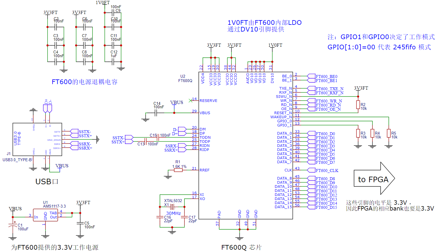 |
|---|
| 图5:FT600 USB 接口电路的参考原理图设计 |
在 FPGA 工程中,另外注意以下几点:
usb_clk频率为 100MHz 。你可以把usb_clk约束为 100MHz,来指导时序分析。实际上,即使不加该约束也不影响正常运行。- fpga_top_example_ft600.sv 中的主时钟 clk 要连在 FPGA 板的晶振上,频率不限,比如 24MHz, 50MHz, 100MHz 均可。
- led 引脚连一颗 LED 灯(不是必须的),它平常保持 1,当发现接收到的数据不是递增的时,会变成 0 并保持一秒。
- 请关注本例 fpga_top_example_ft600.sv 中 ftdi_245fifo 模块的参数配置:
C_DEXP被设为 1,这是因为 FT600 的数据线是 16bit 的。TX_DEXP被设为 3,因此用户发送接口的tx_data信号的宽度是 64bit(这只是本例的取值,你可以根据你的项目需要来修改)。RX_DEXP参数被设为 0,因此用户接收接口的rx_data信号的宽度是 8bit(这只是本例的取值,你可以根据你的项目需要来修改)。
然后你就可以编译工程,步骤略。
我在 python_ft600 文件夹中提供了以下几个 Python 程序,它们会通过 FT600 与 FPGA 进行通信。运行这些程序之前,请确保 FPGA 中下载了步骤2中建立的工程。
| 文件 | 功能 |
|---|---|
| USB_FT600.py | 定义了 USB_FT600_sync245mode 类,实现了 构造函数, close, send, recv 方法,它会被其它文件调用。 |
| usb_rx.py | 简单地试图接收 32 个字节(FPGA 发送,Host-PC 接收) |
| usb_tx.py | 简单地发送 16 个字节(FPGA 接收,Host-PC 发送) |
| usb_rx_rate.py | Host-PC 不断接收大量数据,并统计通信速率 |
| usb_rx_tx_validation.py | 同时进行收发正确性验证,它会不间断地发送和接收。因为配套的 FPGA 程序会发送的是递增数据,所以该程序会验证收到的数据是否连续递增(遇到不连续则警告并退出)。同时该程序也会不断地发递增的数据,FPGA也会验证收到的数据是否连续递增,遇到不连续则把 led 管脚置 0(灯灭)一秒。通常,程序开始运行时灯会灭一秒(因为本次和上次收到的数据大概率不连续),但之后正常情况下不会再灭。 |
- FT232H 芯片资料:http://www.ftdichip.cn/Products/ICs/FT232H.htm
- FT232H 软件示例:http://www.ftdichip.cn/Support/SoftwareExamples/CodeExamples.htm
- FT600 芯片资料:http://www.ftdichip.cn/Products/ICs/FT600.html
- FT600/FT601 软件示例: http://www.ftdichip.cn/Support/SoftwareExamples/FT60X.htm
An FPGA-based controller for FT232H , FT2232H , FT600 , FT601 chips in sync-245-fifo mode, which can realize fast USB communication between FPGA and Host-PC.
sync-245-fifo mode (referred to as 245fifo mode) is the highest speed transmission mode of FTDI's USB series chips. This repository implement a 245fifo controller Verilog module (ftdi_245fifo.sv, see Figure1), providing a streaming transceiver interface for Verilog developers.
In addition, this repository provides supplementary:
- FPGA sample projects,
- FTDI driver installation tutorials,
- Python software library installation tutorials,
- Several Python programs for testing.
 |
|---|
| Figure1 : diagram of ftdi_245fifo.sv |
- Send/Receive scheduling: The interface between the FTDI USB chip and the FPGA is half-duplex. This module schedules the sending and receiving using time-division multiplexing to achieve independent send and receive interface.
- Clock Domain Crossing: The FTDI USB chip has its own clock. This module uses asynchronous FIFO to realize clock domain crossing, so that the send and receive interface can use custom clocks .
- Bit width conversion: The data bit width of the FTDI USB chip is fixed. This module realizes the bit width conversion so that the bit width of the send and receive interface can be customized .
The following table shows the communication rate of the USB upstream (FPGA send, Host-PC receive).
| FT232H or FT2232H | FT600 | FT601 | |
|---|---|---|---|
| USB generation | USB2.0 HS | USB3.0 SS | USB3.0 SS |
| Theoretical | 60MBps | 200MBps | 400MBps |
| Testing | 42MBps | 120MBps | didn't test |
The design code of this library is ftdi_245fifo.sv in the RTL folder, which can be called by FPGA developers to develop their own USB communication applications. Its interface and parameters are shown in Figure2.
 |
|---|
| Figure2 : interface of ftdi_245fifo.sv |
To call this module, you should first determine the value of each Verilog parameter, as shown in the following table:
| parameter | Introduction |
|---|---|
| TX_DEXP | Determines the data width of the user's send interface (that is, the width of tx_data): 0 corresponds to 8bit width, 1 corresponds to 16bit width, 2 corresponds to 32bit width, 3 corresponds to 64bit width, and so on. It can be set arbitrarily according to actual requirement and is not limited by the selected USB chip. |
| TX_AEXP | Determines the depth of the user's send buffer, depth=2^TX_AEXP. The default is 10 (that is, the default depth is 1024). If the FPGA BRAM is larger, it can be set larger to improve burst performance. |
| RX_DEXP | Determines the data width of the user's receive interface (that is, the width of rx_data): 0 corresponds to 8bit width, 1 corresponds to 16bit width, 2 corresponds to 32bit width, 3 corresponds to 64bit width, and so on. It can be set arbitrarily according to actual requirement and is not limited by the selected USB chip. |
| RX_AEXP | Determines the depth of the user's receive buffer, depth=2^RX_AEXP. The default is 10 (that is, the default depth is 1024). If the FPGA BRAM is larger, this item can be set larger to improve burst performance. |
| C_DEXP | Determines the width of the USB data signal (that is, usb_data): 0 corresponds to 8bit width, 1 corresponds to 16bit width, 2 corresponds to 32bit width, and 3 corresponds to 64bit width. It should be set according to the selected USB chip: 0 for FT232H, 1 for FT600, and 2 for FT601. |
rstn_async is the global asynchronous reset of the module, 0 means reset, 1 means release reset. This signal can be directly set to 1'b1, or connected to the global reset signal.
usb_rxf, usb_txe, usb_oe, usb_rd, usb_wr, usb_data and usb_be should be constrained to the pins of the FPGA and connected to the corresponding pins of the FTDI USB chip. Note the following:
- When the FTDI USB chip works in 245fifo mode, see the chip datasheet for its pin definations (take FT232H as an example, see FT232H DataSheet page 9).
usb_beis the byte enable signal, only FT600 and FT601 chips have this signal. For FT232H and FT2232H, ignore it.- The waveform of these pins is maintained by the module. You don't need to pay attention about it. If you are interested, you can run [RTL simulation](#Module Simulation).
This module has a built-in send buffer. The developer needs to provide a tx_clk clock and operate the three signals tx_valid, tx_ready, tx_data in this clock domain to send data from the FPGA to the sendbuffer. (When the receiving program starts on the Host-PC, the data in the sending buffer will be sent to the PC automatically). Note the following:
- The frequency of
tx_clkis not limited,tx_valid,tx_ready,tx_datasignals should be updated or sampled on the rising edge oftx_clk. - When
tx_valid=1, it means that the user wants to send a data to the send buffer. Meanwhile,tx_datashould produce a valid data. - When
tx_ready=1, the module is ready to accept a data. Whentx_ready=0, the send buffer is temporarily full and no more data can be accepted. tx_validandtx_readyare a pair of handshake signals. When both are 1,tx_datais successfully written to the trasmit buffer.
Take the following waveform as an example, in this waveform, the user interface sends 3 data: D1, D2, D3.
-
In the 1st and 2nd cycles, the user sets
tx_valid=0, so it is temporarily idle and no data is sent. -
In the 3rd cycle, the user wants to send D1, so it set
tx_valid=1, this cycletx_ready=1, indicating that D1 is sent to buffer successfully. -
In the 4th, 5th, 6th, and 7th cycles, the user wants to send D2, so it set
tx_valid=1, but the 4th, 5th, 6th cyclestx_ready=0cause the transmission to temporarily fail until the 7th cycletx_ready=1is sent successfully. -
In the 8th and 9th cycles, the user sets
tx_valid=0, so it is temporarily idle and no data is sent. -
In the 10th cycle, the user wants to send D3, so it set
tx_valid=1, this cycletx_ready=1, indicating that D3 is sent successfully. -
cycle       1     2     3     4     5     6     7     8     9     10    11
          _    __    __    __    __    __    __    __    __    __    __    __
 clk       \__/  \__/  \__/  \__/  \__/  \__/  \__/  \__/  \__/  \__/  \__/  \
                      _____________________________             _____
tx_valid  ___________/                             \___________/     \________
          _________________                   ________________________________
tx_ready                   \_________________/
                      _____ _______________________             _____
tx_data   XXXXXXXXXXXX__D1_X___________D2__________XXXXXXXXXXXXX__D3_XXXXXXXXX
This module has a built-in receive buffer, the developer needs to provide a rx_clk clock, and operate the three signals rx_valid, rx_ready, rx_data in this clock domain to fetch out the temporary buffered data that come from the Host-PC. It has a same waveform as the user send interface, but in the opposite direction. Note the following:
- The frequency of
rx_clkis not limited (of course, it can be as same clock astx_clk),rx_valid,rx_ready,rx_datasignals should be updated or sampled on the rising edge ofrx_clk. - When
rx_valid=1, it means that the module wants to send a data to the user. Meanwhile, a valid data appeared onrx_data. Whenrx_valid=0, the receive buffer is empty and no more data can be fetched out. - When
rx_ready=1, it means that the user is ready to fetch out a data. rx_validandrx_readyare a pair of handshake signals. When both are 1,rx_datais successfully fetched out from the receive buffer.
The waveform of the user receive interface is similar to that of the user sending interface (the only difference is the opposite direction), so the waveform diagram will not be illustrated here.
If you are curious about the design details of the ftdi_245fifo.sv module, or want to know the operation waveform of the FTDI USB chip in 245fifo mode, you can run the RTL simulation.
Simulation related files are in the SIM folder, where:
- tb_ftdi_245fifo.sv is the testbench for ftdi_245fifo.sv, it simulates the behavior of a simple FT232H and exchanges data with ftdi_245fifo.sv.
- tb_ftdi_245fifo_run_iverilog.bat is the command script to run the iverilog simulation.
Before using iverilog for simulation, you need to install iverilog , see: iverilog_usage
Then double-click tb_ftdi_245fifo_run_iverilog.bat to run simulation, and then you can open the generated dump.vcd file to view the waveform.
FT232H is a USB2.0 High Speed communication chip with a theoretical rate of 60MBps. In this demo, the FPGA communicates with Host-PC through FT232H.
Note: This demo also applies to FT2232H (you need to work around it yourself), because FT2232H is highly similar to FT232H, channel A of FT2232H can be configured to be the exact same 245fifo interface as FT232H.
Please follow the instructions in FTD2XX_guide.md to install the FTD2XX driver and Python FTD2XX library on your Host-PC (Windows system).
Build an FPGA project and add the following Verilog source files:
- fpga_top_example_ft232h.sv in the RTL folder: as the top module of the project.
- ftdi_245fifo.sv , stream_async_fifo.sv , stream_wtrans.sv in the RTL folder: they will be called by the top module.
Then, please make pin constraints in the FPGA project. Specifically, you need to check the schematic of your FPGA board (or the supporting materials of the development board) to understand which FT232H pin should connected to which FPGA pin; then, constraint the signals of the top layer of the FPGA project (that is, fpga_top_example_ft232h.sv) to the corresponding FPGA pin number. The correspondence is shown in the following table (this table is simplified from FT232H DataSheet page 9):
| FT232H pin | FT232H pin name | FT232H pin name (in 245fifo mode) | signal name in top module |
|---|---|---|---|
| 13 | ADBUS0 | D0 | usb_data[0] |
| 14 | ADBUS1 | D1 | usb_data[1] |
| 15 | ADBUS2 | D2 | usb_data[2] |
| 16 | ADBUS3 | D3 | usb_data[3] |
| 17 | ADBUS4 | D4 | usb_data[4] |
| 18 | ADBUS5 | D5 | usb_data[5] |
| 19 | ADBUS6 | D6 | usb_data[6] |
| 20 | ADBUS7 | D7 | usb_data[7] |
| 21 | ACBUS0 | RXF# | usb_rxf |
| 25 | ACBUS1 | TXE# | usb_txe |
| 26 | ACBUS2 | RD# | usb_rd |
| 27 | ACBUS3 | WR# | usb_wr |
| 28 | ACBUS4 | SIWU# | usb_siwu * (=1) |
| 29 | ACBUS5 | CLKOUT | usb_clk |
| 30 | ACBUS6 | OE# | usb_oe |
| 31 | ACBUS7 | PWRSAV# | usb_pwrsav * (=1) |
| 34 | RESET# | RESET# | usb_resetn * (=1) |
*Note : SIWU#, PWRSAV# and RESET# in the above table are actually always pulled to high (you can also see that they are assigned 1 in fpga_top_example_ft232h.sv). Some boards directly use resistors to pull-up them without connecting them to the FPGA, in this case, you don't need to constrain these pins and simply comment out the statements related to them in fpga_top_example_ft232h.sv.
Note : For FT2232H, please refer to FT2232H DataSheet page 9.
If you want to draw the FT232H PCB by yourself, please refer to Figure3.
 |
|---|
| Figure3 : Example schematic design of FT232H USB interface circuit. |
In the FPGA project, please note:
usb_clkfrequency is 60MHz. You can constrainusb_clkto 60MHz to guide timing analysis. In fact, even if the constraint is not imposed, it will not affect normal operation.- The main clock
clkin fpga_top_example_ft232h.sv should be connected to the crystal oscillator of the FPGA board, and the frequency is not limited, such as 24MHz, 50MHz, 100MHz. - The led pin is connected to an LED light (not necessary), it usually remains 1, when it is found that the received data is not incremented, it will become 0 and remain for one second.
- Please pay attention to the parameter configuration of the ftdi_245fifo module in fpga_top_example_ft232h.sv in this example:
C_DEXPis set to 0, this is because the data line of FT232H is 8bit.TX_DEXPis set to 3, so the width of thetx_datasignal of the user sending interface is 64bit (this is just the value of this example, you can modify it according to your project needs).- The
RX_DEXPparameter is set to 0, so the width of therx_datasignal of the user receiving interface is 8bit (this is just the value of this example, you can modify it according to your project needs).
Then you can compile the project, this step is omitted.
For each FT232H chip, it needs to be programmed to 245fifo mode when it is used for the first time. Each FT232H chip only needs to be programmed once, because there is an EEPROM chip on the periphery of the FT232H to permanently save the configuration, and it does not need to be programmed again every time it is used (unless you program it to another mode).
First go to the FT_Prog download page to download and install FT_Prog software. Then do the following steps:
- Plug the USB of FT232H to the computer, and unplug all other FTDI USB chip or device (including FPGA downloaders, because some FPGA downloaders, such as Xilinx Digilent downloaders, are implemented by the FT2232H chip, if the program inside the downloader is overwritten, your downloader will be useless).
- Open FT_Prog software.
- As shown in Figure4, click Scan and Parse (the icon is a small magnifying glass) to scan all FTDI chips plugged into the computer and find the corresponding chip of FT232H.
- In the property tree below FT232H, expand level by level, find and click "Hardware" .
- Select 245 FIFO mode on the right.
- Click Program (the icon is a small lightning) in the upper toolbar.
- A confirmation window pops up, click Program. Program to FT232H.
- After programming, you need to re-plug the USB to let this configuration takes effect.
 |
|---|
| Figure4 : Program FT232H chip to 245fifo mode. |
I provide the following Python programs in the python_ft232h folder that will communicate with the FPGA through the FT232H. Before running these programs, please make sure that the FT232H has been programmed into 245fifo mode according to step3, and the FPGA project created in step2 has been programed to the FPGA.
| File Name | Function |
|---|---|
| USB_FT232H.py | Defines the USB_FT232H_sync245mode class, implements the constructor, close, send, recv methods, which will be called by the following files. |
| usb_rx.py | Simply trying to receive 32 bytes (FPGA sends, Host-PC receives) |
| usb_tx.py | Simply send 16 bytes (FPGA receive, Host-PC send) |
| usb_rx_rate.py | Host-PC continuously receives a large amount of data and statistic the communication rate. |
| usb_rx_tx_validation.py | Test sending and receiving simutinously. It will send and receive without interruption. Because the FPGA program sends incremental data, this python program will verify that the received data is continuously incremented. Meanwhile, the program will send incremental data, and the FPGA will also verify whether the received data is continuously increasing. If it is discontinuous, it will set the led pin to 0 (light off) for 1 second. Usually, the light will go off for one second when the program starts running (because the data received this time and the last time are definitely not continuous), but it will not go off under normal circumstances after that. |
The FT600 is a USB3.0 Super Speed communication chip with a theoretical rate of 200MBps. In this example, the FPGA communicates with the Host-PC through FT600.
Please follow the instructions in FTD3XX_guide.md to install the FTD3XX driver and Python FTD3XX library on your Host-PC (Windows system).
Build an FPGA project and add the following Verilog source files:
- fpga_top_example_ft600.sv in the RTL folder: as the top module of the project.
- ftdi_245fifo.sv , stream_async_fifo.sv , stream_wtrans.sv in the RTL folder: they will be called by the top module.
Then, please make pin constraints in the FPGA project. Specifically, you need to check the schematic of your FPGA board (or the supporting materials of the development board) to understand which FT600 pin should connected to which FPGA pin; then, constraint the signals of the top layer of the FPGA project (that is, fpga_top_example_ft600.sv) to the corresponding FPGA pin number. The correspondence is shown in the following table (this table is simplified from FT600 DataSheet page 7-10):
| FT600 pin number | FT600 pin name | signal name in top module |
|---|---|---|
| 33 | DATA_0 | usb_data[0] |
| 34 | DATA_1 | usb_data[1] |
| 35 | DATA_2 | usb_data[2] |
| 36 | DATA_3 | usb_data[3] |
| 39 | DATA_4 | usb_data[4] |
| 40 | DATA_5 | usb_data[5] |
| 41 | DATA_6 | usb_data[6] |
| 42 | DATA_7 | usb_data[7] |
| 45 | DATA_8 | usb_data[8] |
| 46 | DATA_9 | usb_data[9] |
| 47 | DATA_10 | usb_data[10] |
| 48 | DATA_11 | usb_data[11] |
| 53 | DATA_12 | usb_data[12] |
| 54 | DATA_13 | usb_data[13] |
| 55 | DATA_14 | usb_data[14] |
| 56 | DATA_15 | usb_data[15] |
| 2 | BE_0 | usb_be[0] |
| 3 | BE_1 | usb_be[1] |
| 43 | CLKOUT | usb_clk |
| 5 | RXF_N | usb_rxf |
| 4 | TXE_N | usb_txe |
| 9 | OE_N | usb_oe |
| 8 | RD_N | usb_rd |
| 7 | WR_N | usb_wr |
| 6 | SIWU_N | usb_siwu * (=1) |
| 10 | RESET_N | usb_resetn * (=1) |
| 11 | WAKEUP_N | usb_wakeupn ** (=0) |
| 12 | GPIO0 | usb_gpio0 ** (=0) |
| 13 | GPIO1 | usb_gpio1 ** (=0) |
*Note : SIWU_N and RESET_N in the above table are actually always pulled to high (you can also see that they are assigned 1 in fpga_top_example_ft600.sv). Some boards directly use resistors to pull-up them without connecting them to the FPGA, in this case, you don't need to constrain these pins and simply comment out the statements related to them in fpga_top_example_ft600.sv.
**Note : WAKEUP_N, GPIO0 and GPIO1 in the above table are actually always pulled to GND (you can also see that they are assigned 0 in fpga_top_example_ft600.sv). Some boards directly use resistors to pull-down them without connecting them to the FPGA, in this case, you don't need to constrain these pins and simply comment out the statements related to them in fpga_top_example_ft600.sv.
If you want to draw the FT600 PCB by yourself, please refer to Figure5.
 |
|---|
| Figure3 : Example schematic design of FT600 USB interface circuit. |
In the FPGA project, please note:
usb_clkfrequency is 100MHz. You can constrainusb_clkto 100MHz to guide timing analysis. In fact, even if the constraint is not imposed, it will not affect normal operation.- The main clock
clkin fpga_top_example_ft600.sv should be connected to the crystal oscillator of the FPGA board, and the frequency is not limited, such as 24MHz, 50MHz, 100MHz. - The led pin is connected to an LED light (not necessary), it usually remains 1, when it is found that the received data is not incremented, it will become 0 and remain for one second.
- Please pay attention to the parameter configuration of the ftdi_245fifo module in fpga_top_example_ft600.sv in this example:
C_DEXPis set to 1, this is because the data line of FT600 is 16bit.TX_DEXPis set to 3, so the width of thetx_datasignal of the user sending interface is 64bit (this is just the value of this example, you can modify it according to your project needs).- The
RX_DEXPparameter is set to 0, so the width of therx_datasignal of the user receiving interface is 8bit (this is just the value of this example, you can modify it according to your project needs).
Then you can compile the project, this step is omitted.
I provide the following Python programs in the python_ft600 folder that will communicate with the FPGA through FT600. Before running these programs, please make sure that the FPGA project created in step2 has been programed to the FPGA.
| File Name | Function |
|---|---|
| USB_FT600.py | Defines the USB_FT600_sync245mode class, implements the constructor, close, send, recv methods, which will be called by the following files. |
| usb_rx.py | Simply trying to receive 32 bytes (FPGA sends, Host-PC receives) |
| usb_tx.py | Simply send 16 bytes (FPGA receive, Host-PC send) |
| usb_rx_rate.py | Host-PC continuously receives a large amount of data and statistic the communication rate. |
| usb_rx_tx_validation.py | Test sending and receiving simutinously. It will send and receive without interruption. Because the FPGA program sends incremental data, this python program will verify that the received data is continuously incremented. Meanwhile, the program will send incremental data, and the FPGA will also verify whether the received data is continuously increasing. If it is discontinuous, it will set the led pin to 0 (light off) for 1 second. Usually, the light will go off for one second when the program starts running (because the data received this time and the last time are definitely not continuous), but it will not go off under normal circumstances after that. |
- FT232H chip:http://www.ftdichip.cn/Products/ICs/FT232H.htm
- FT232H software example:http://www.ftdichip.cn/Support/SoftwareExamples/CodeExamples.htm
- FT600 chip:http://www.ftdichip.cn/Products/ICs/FT600.html
- FT600/FT601 software example: http://www.ftdichip.cn/Support/SoftwareExamples/FT60X.htm
-CAD09D.svg)


