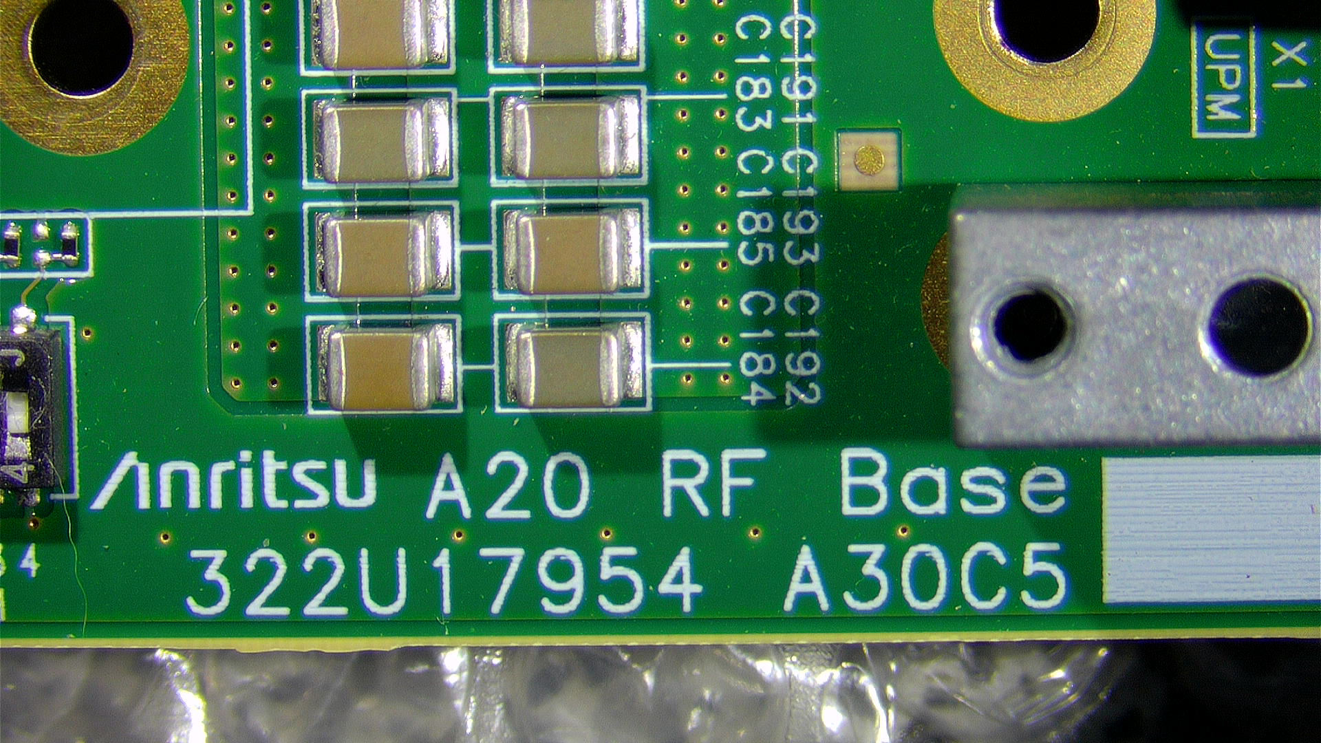
Reverse-engeneer and document Nyanritsu 322U17954 RF Base(board) in order to play with Intel Stratix 10 and Xilinx MPSoC FPGAs, as well with multi-gigabit JESD204B ADC and DAC.
Unknown at the moment; most likely, it was a part of Nyanritsu's 4G test & measurement equipment that went into recycling for some reason. Was bougth on Ebay from an e-waste company for ~200USD.
The only hunch we have so far is https://www.linkedin.com/in/anthony-curran-79a7474:
Anritsu, Lead DSP Consultant
Dates Employed May 2018 – Apr 2020
Employment Duration 2 yrs
Location Acton, Massachusetts, United States
5G-NR Radio Channel Emulation.
3GPP Algorithm Development and Implementation.
Xilinx MPSoC, Intel/Altera Stratix-10 FPGA
Matlab, C++, System Verilog
- Intel Stratix 10 FPGA (1SG280LU3F50E3XG, 2.75M LEs)
- Xilinx UltraScale+ MPSoC FPGA (XCZU9EG, 700K system logic cells, quad Cortex-A53, dual Cortex-R5F)
- 2x DDR3 SO-DIMM slots for S10
- 1x DDR3 SO-DIMM slot for MPSoC
- 4x SAMTEC Firefly connectors
- 2x AD9162 16b 12GSPS JESD204B DAC
- 1x AD9208 14b 3GSPS JESD204B ADC
- Marvel 88E1111 Gigabit PHY
- Fairly sophisticated RF section
- 4 SAMTEC Firefly PCB connectors (12x configuration); 2x Firefly 12x optics modules are typically included with each board (with fiber ribbon cut really short)
- Erni 973028 (
X3,"ZD") backplane connector (for unknown number of XCVR lanes) - TE 1-1746992-1 (
X2,"HM") backplane connector (at least for GigE, external clocks, control) - SAMTEC Q Strip series (possibly, QSH-060-01-F-D) (
X23,"Debug") 120-pin debug connector - 2x (unknown type) "RF mezzanine connectors" (as described by the seller), typically broken, labelled as
"RF{1,2}_INT" - 2x (unknown type) 20-pin I/O connectors, labelled as
"RF{1,2}_EXT"
The board is powered from a two +12V DC sources - +12VD and +12VA via main power connector "UPM" (TE 5646955-2).
You can supply the 12V power from a single source by soldering wires to +12VD (X58), +12VA (X57) and GND (X56) SMD test terminals on the bottom side, near the power connector.
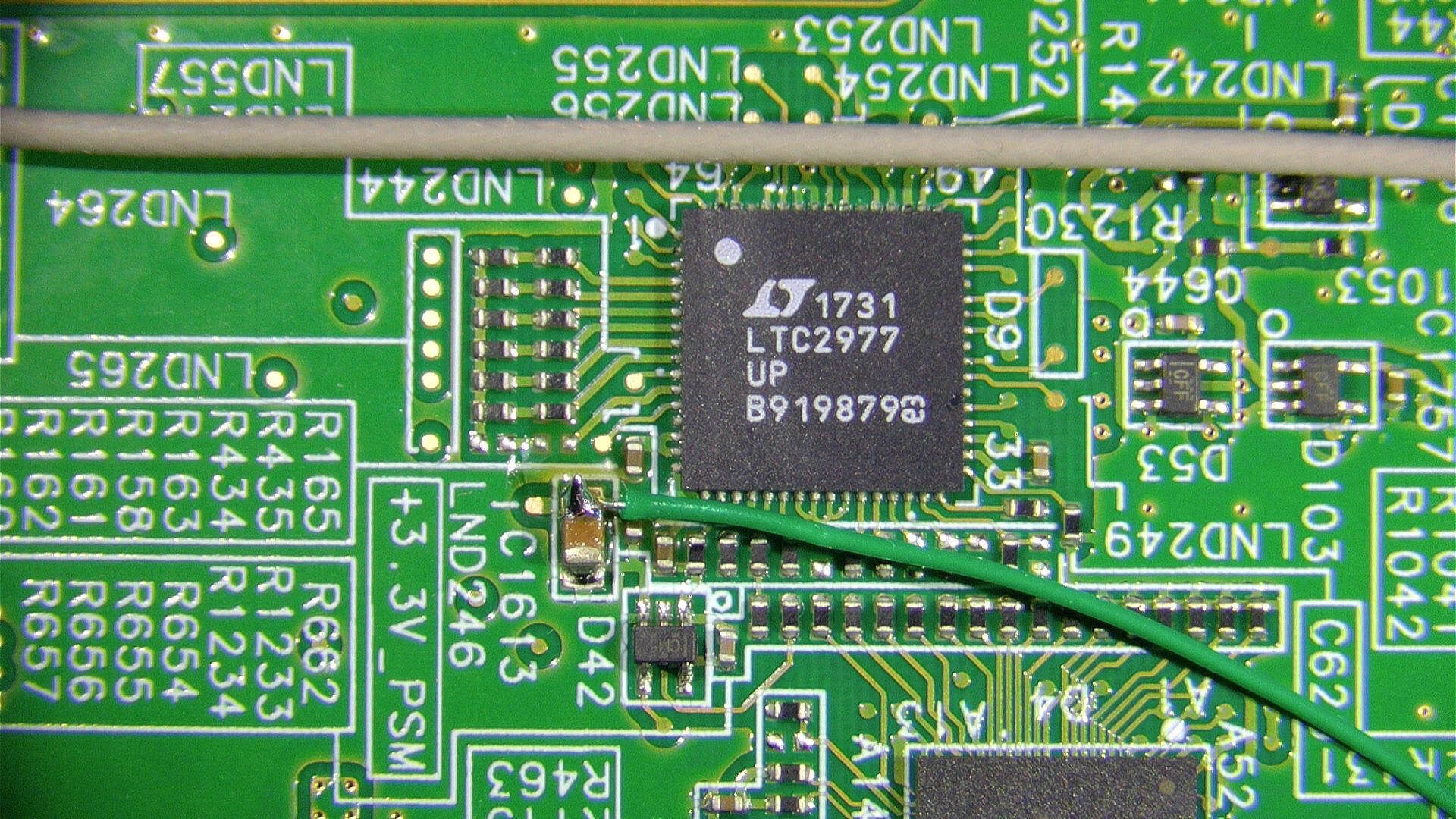
The powering-up and rail sequencing procedure is controlled by Linear LTC2977 controller (D9, also referred as PSM; bottom side, near backplane connectors). It's powered from a standby rails and won't power up the board, unless there's a 3V3 enable signal coming from the chassis via "UPM" connector.
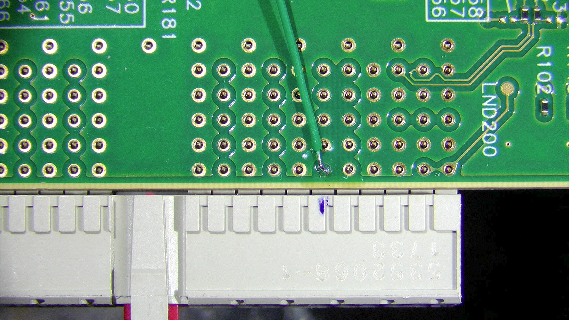
You can connect +3.3_PSM rail (one of the C1613 terminals, or from LND246 testpoint) to the enable signal (A20 pin on X2 connector).
Soldering point for +3.3_PSM rail:

Soldering point for enable signal on the X2 ("HM") connector:

The board also have X18 ("PSM") connector to hook up DC1613 USB-to-I2C/SMBus/PMBus Controller from Linear.
For Stratix 10 use X21 ("FPGA_JTAG") connector.
For MPSoC use X19 ("PS_JTAG") connector. By default, the board is set up to boot MPSoC from the MicroSD card, which is typically not present. You can switch MPSoC boot mode to JTAG using S1 ("PS_MODE") switch.


