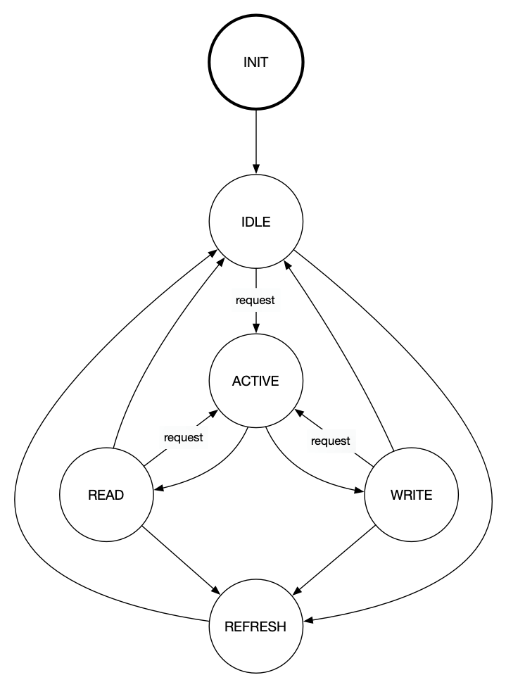
Because synchronous dynamic RAM (SDRAM) has complex timing and signalling requirements, a memory controller is necessary to avoid having to deal with the nitty-gritty details when reading or writing to memory. Its job is to hide the complexity of things like row and column addressing, precharging, and refreshing. Instead it lets us treat SDRAM just like plain old static memory.
This SDRAM controller provides a symmetric 32-bit synchronous read/write interface for a 16Mx16-bit SDRAM chip (e.g. AS4C16M16SA-6TCN, IS42S16400F, etc.).
Even though the SDRAM chip only has a 16-bit data bus, the controller uses a 32-bit data bus because it is more efficient to burst multiple words from the SDRAM than it is to do individual reads and writes.
| name | direction | description |
|---|---|---|
| reset | input | resets the SDRAM controller when asserted |
| clk | input | clock |
| addr | input | address bus |
| data | input | input data bus |
| we | input | write enable |
| req | input | requests a read or write operation when asserted |
| ack | output | asserted when a request is accepted by the SDRAM controller |
| valid | output | asserted when there is valid data on the output data bus |
| q | output | output data bus |
The reset signal can be used to reset the internal state machine for the SDRAM controller.
The clk signal is the system clock used by the SDRAM controller.
Ideally, it should be different to the SDRAM clock (i.e. the clock for the actual SDRAM chip). By adjusting the phase relationship so that the SDRAM clock leads the system clock, we can ensure that the SDRAM output signals arrive in time to meet our timing constraints.
The addr signal should be set to the address of the memory location being accessed.
The data signal should be set to the 32-bit value to be written to the memory location at the given address.
The we signal should be asserted when you want to write to the SDRAM. It should be asserted together with the req signal.
The req signal should be asserted when you want to read or write to the SDRAM. When making a request, the req, we, addr, and data signals should not be changed until the request has been acknowledged.
The ack signal is asserted by the SDRAM controller when a request has been acknowledged.
The valid signal is asserted by the SDRAM controller when there is valid data on the output data bus.
The q signal is set to the last 32-bit word read from the SDRAM. The data on the output bus is only valid while the valid signal is asserted.
The SDRAM controller allows read operations to be performed using a simple interface.
Read requests can be chained so that a new read operation can be requested before the current operation has completed. Using this strategy, we can read any number of words from the SDRAM without wasting clock cycles, thus using the maximum available bandwidth of the SDRAM.
The following example describes how to read two 32-bit words using the SDRAM controller. This method can be used to read any number of words:
- Write the address to the
addrbus. - Request a read operation by deasserting the
wesignal and asserting thereqsignal. - Wait for the
acksignal to be asserted. This means that the read request has been acknowledged, and a read operation has begun. - Write another address to the
addrbus. - Wait for the
validsignal to be asserted. This means that the first read request has been completed and the data is available on the data bus. - Read the value on the
qdata bus. - Wait for
acksignal to be asserted. This means that the second read request has been acknowledged, and a read operation has begun. - Deassert the
reqsignal when we're done making requests. - Wait for the
validsignal to be asserted. This means that the second read request has been completed and the data is available on the data bus. - Read the value on the
qdata bus.
The SDRAM controller handles write operations similarly to read operations.
Write requests can also be chained, so that a new write operation can be requested before the current operation has completed.
The following example describes how to write two 32-bit words using the SDRAM controller. This method can be used to write any number of words:
- Write an address to the
addrbus and a value to the data bus. - Request a write operation by asserting the
weandreqsignals. - Wait for the
acksignal to be asserted. This means that the write request has been acknowledged, and a write operation has begun. - Write another address to the
addrbus and a value to the data bus. - Wait for
acksignal to be asserted. This means that the second write request has been acknowledged, and a write operation has begun. - Deassert the
weandreqsignals when we're done making requests.
This project is licensed under the MIT licence. See the LICENCE file for more details.


