ECL 312: CMOS Design
A Project Report on: 2-bit Comparator Using CMOS
Submitted By:
Ayush Ambatkar (BT22ECI005)
Contributors:
Jjateen Gundesha (BT22ECI002) – SPICE Netlist Creation
Under the Guidance of:
Prof. Paritosh Peshwe
Department of Electronics and Communication
The 2-bit digital comparator project presents a CMOS-based circuit designed to compare two 2-bit binary inputs, A and B, and output three signals indicating their relationship: whether A is less than, equal to, or greater than B. The circuit was designed using CMOS gates such as AND, OR, XNOR, and inverters to achieve accurate and power-efficient performance. The netlist provides a foundational structure for simulating the circuit and guiding its layout.
- Design a 2-bit CMOS comparator.
- Generate three output signals indicating the comparison result (
A < B,A = B,A > B). - Implement the circuit using basic CMOS gates.
- Verify the circuit's operation in WinSpice.
- Develop a layout suitable for fabrication using Microwind.
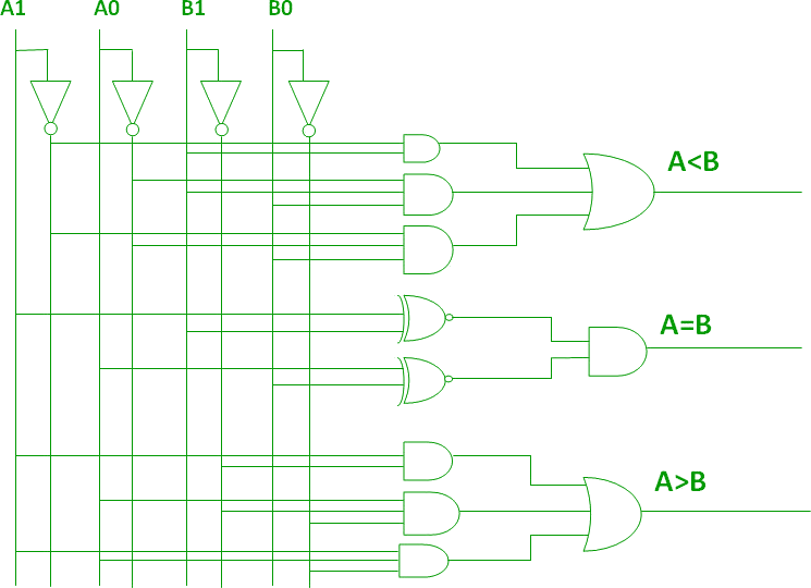
The comparator circuit receives two 2-bit binary inputs, A (A1A0) and B (B1B0), and produces the following outputs:
A < B: Active whenBis greater thanA.A = B: Active when both inputs are equal.A > B: Active whenAis greater thanB.
- Equality (
A = B): Achieved using XNOR gates for each bit pair and an AND gate to combine the results. - Less Than (
A < B): Implemented with AND gates to evaluate conditions likeA1 < B1or, ifA1 = B1,A0 < B0. - Greater Than (
A > B): Uses AND gates for scenarios whereAhas higher bits thanB.
The SPICE netlist facilitates simulation in WinSpice for circuit functionality verification.
***2 Bit Comparator***
.model nmod nmos level=54 version=4.7
.model pmod pmos level=54 version=4.7
.ic v(13)=0 v(17)=0 v(20)=0
* Inverter Subcircuit
.subckt inverter in vdd out
M1 out in 0 0 nmod w=100u l=10u
M2 out in vdd vdd pmod w=200u l=10u
Cout out 0 1p
.ends

* AND Gate Subcircuit
.subckt and2 a b output vdd
M1 out a n1 n1 nmod w=100u l=10u
M2 n1 b 0 0 nmod w=100u l=10u
M3 out a vdd vdd pmod w=100u l=10u
M4 out b vdd vdd pmod w=100u l=10u
Xout out vdd output inverter
.ends

* 3 i/p AND Gate Subcircuit
.subckt and3 a b c output vdd
M1 out a n1 n1 nmod w=100u l=10u
M2 n1 b n2 n2 nmod w=100u l=10u
M3 n2 c 0 0 nmod w=100u l=10u
M4 out a vdd vdd pmod w=100u l=10u
M5 out b vdd vdd pmod w=100u l=10u
M6 out c vdd vdd pmod w=100u l=10u
Xout out vdd output inverter
.ends

* NAND Gate Subcircuit
.subckt nand2 a b out vdd
M1 out a n1 n1 nmod w=100u l=10u
M2 n1 b 0 0 nmod w=100u l=10u
M3 out a vdd vdd pmod w=200u l=10u
M4 out b vdd vdd pmod w=200u l=10u
.ends

* OR Gate Subcircuit
.subckt or2 a b out vdd
M1 n1 b 0 0 nmod w=100u l=10u
M2 n1 a 0 0 nmod w=100u l=10u
M3 n1 b n2 n2 pmod w=200u l=10u
M4 n2 a vdd vdd pmod w=200u l=10u
Xa_inv n1 vdd out inverter
.ends

* 3 i/p OR Gate Subcircuit
.subckt or3 a b c out vdd
M1 n1 b 0 0 nmod w=100u l=10u
M2 n1 a 0 0 nmod w=100u l=10u
M3 n1 c 0 0 nmod w=100u l=10u
M4 n1 c n2 n2 pmod w=200u l=10u
M5 n2 b n3 n3 pmod w=200u l=10u
M6 n3 a vdd vdd pmod w=200u l=10u
Xa_inv n1 vdd out inverter
.ends

* NOR Gate Subcircuit
.subckt nor2 a b out vdd
M1 out b 0 0 nmod w=100u l=10u
M2 out a 0 0 nmod w=100u l=10u
M3 out b n2 n2 pmod w=200u l=10u
M4 n2 a vdd vdd pmod w=200u l=10u
.ends

.subckt xnor a b out ab bb vdd
M1 out ab n1 n1 nmod w=100u l=10u
M2 out a n2 n2 nmod w=100u l=10u
M3 n1 b 0 0 nmod w=100u l=10u
M4 n2 bb 0 0 nmod w=100u l=10u
M5 out ab n3 n3 pmod w=200u l=10u
M6 out b n3 n3 pmod w=200u l=10u
M7 n3 a vdd vdd pmod w=200u l=10u
M8 n3 bb vdd vdd pmod w=200u l=10u
.model nmod nmos level=54 version=4.7
.model pmod pmos level=54 version=4.7
.ends

vdd 9 0 dc 5v
Va0 1 0 dc 0v
Vb0 2 0 dc 0v
Va1 3 0 dc 5v
Vb1 4 0 dc 5v
Xa0i 1 9 5 inverter
Xb0i 2 9 6 inverter
Xa1i 3 9 7 inverter
Xb1i 4 9 8 inverter
*a<b at 13*
xalb 7 4 10 9 and2
xallb 5 2 4 11 9 and3
xalllb 2 5 7 12 9 and3
xalessb 10 11 12 13 9 or3
*a>b at 17*
xagb 3 8 14 9 and2
xaggb 1 3 6 15 9 and3
xagggb 1 6 8 16 9 and3
xagreatb 14 15 16 17 9 or3
*a=b at 20*
xaeb 3 4 18 7 8 9 xnor
xaeeb 1 2 19 5 6 9 xnor
xaequalb 18 19 20 9 and2

.tran 0.1m 400m
.control
run
plot v(13) v(17) v(20)
.endc
.end
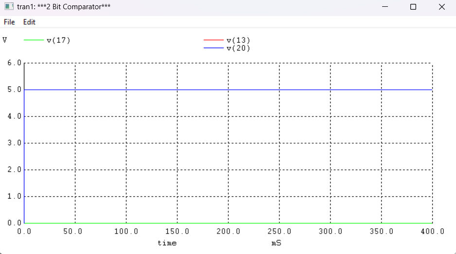
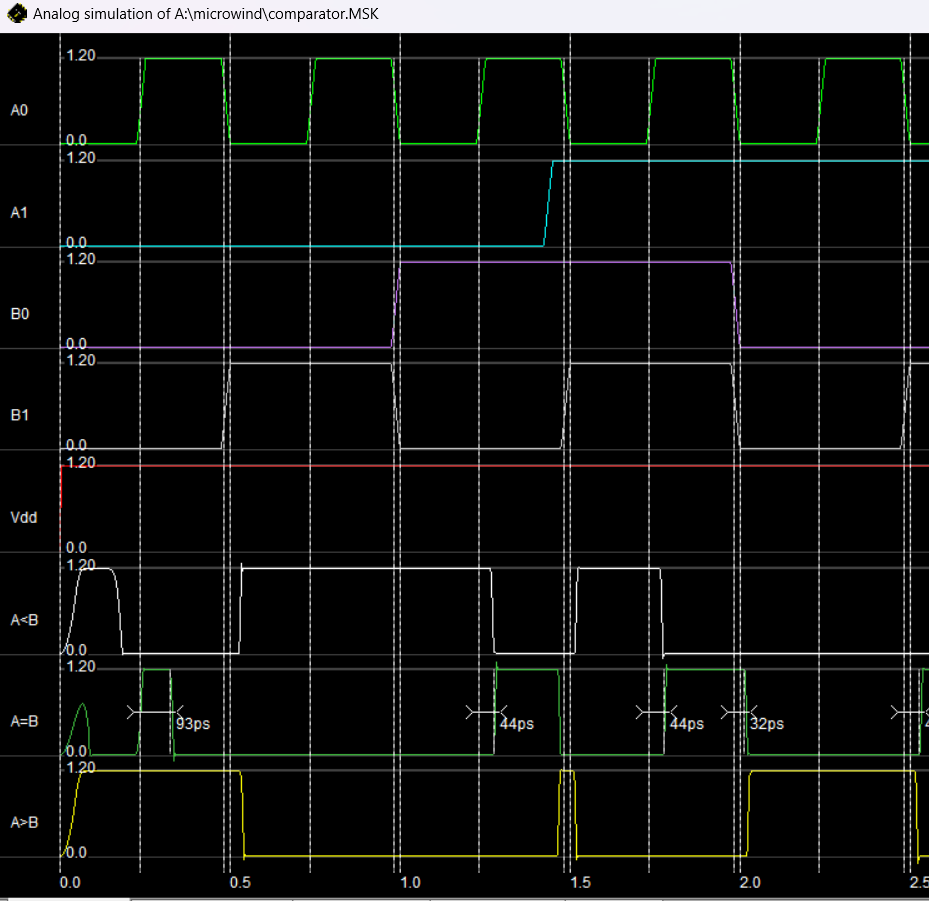
The SPICE simulation was conducted in WinSpice, showing successful verification of the comparator's functionality.
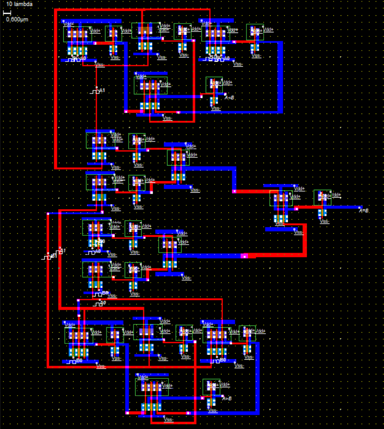
The layout was designed using Microwind, adhering to CMOS design rules for a compact and efficient circuit.
- Threshold Detection: Used in sensors for comparing data against set thresholds.
- Control Systems: Essential for decision-making in microcontrollers.
- Sorting Operations: Helps in digital circuits for selecting smaller numbers.
- Binary Counting: Useful in circuits for determining specific binary values.
- Alarm Systems: Triggers alerts when conditions are met.
-
Power Consumption:
- Challenge: High power usage due to multiple gates.
- Solution: Implemented CMOS technology to reduce static power consumption and optimized transistor sizing.
-
Area Optimization:
- Challenge: Large layout area due to numerous gates.
- Solution: Shared logic gates and compact layout planning minimized the area.
-
Signal Integrity and Noise:
- Challenge: Potential signal interference.
- Solution: Adequate spacing and grounding for noise reduction.
The 2-bit CMOS comparator was successfully designed, simulated, and verified. Key highlights include:
- Accurate comparison for two 2-bit inputs.
- Power efficiency and compact design using CMOS logic.
- Challenges such as power and area optimization were effectively addressed.
- Extend the design to handle 8-bit inputs.
- Optimize for lower power consumption.
- Implement error correction features.
- M. Beiser, "Low Power CMOS Circuits," IEEE Journal of Solid-State Circuits.
- Cadence Virtuoso, "Custom IC and PCB Design."
- Microwind, "CMOS Layout & Simulation Software."


