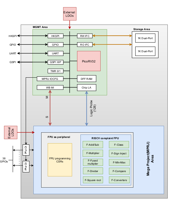
A floating-point unit (FPU), also referred to as numeric co-processor, is a dedicated processing unit that manipulates numbers more quickly than the basic microprocessor circuit. The FPU does this by means of instructions that focus entirely on large mathematical operations such as addition, subtraction, multiplication, or division etc. The F-extension added in user project area, also referred to as FPU is capable to perform floating point addition, subtraction, multiplication, division, square-root and fused multiplication.The block diagram is shown in figure 1.1.
Figure 1.1: Integration of FPU with Caravel SoC
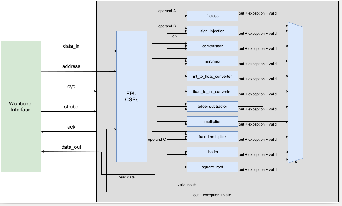
The designed floating-point unit (FPU) is fully compliant with the IEEE-754 standard. It flags all five exceptions explained in subsection xx during result calculation as guided by IEEE-754 spec and has support to round result as per the five rounding modes. Additionally support for dynamic rounding is also added as indicated in RISC-V specifications. The rounding modes are explained in table 1.1. For being compliant with RISC-V F-Extension the unit is capable of performing basic arithmetic operations like comparison, addition, subtraction and multiplication. Moreover, the support for certain complex operations like division, square root of a number and computation of fused multiply-add. Certain other computational operations like integer to float conversion, float to integer conversion, computation of minimum and maximum of the two numbers along with sign injection is added. Caravel SoC core acts as a Wishbone master providing IP with control signals like data, address, cycle and strobe. The signals write FPU CSRs (explained in section 1.2.1) are decoded to provide information including operand A, operand B and operand C. Additionally, the operation that is to be performed and the rounding mode to be used are also provided. The selected module performs operation and the output result is written to an FPU CSR along with the exceptions flagged. The result and exceptions are then forwarded by wb_s to the core when requested.
Figure 1.2: Interface of FPU with wishbone interface
| Rounding Mode | Abbreviation | Encoding |
| Round to Nearest, ties to Even | RNE | 000 |
| Round towards Zero | RTZ | 001 |
| Round Down (towards - inf) | RDM | 010 |
| Round Up (towards + inf) | RUP | 011 |
| Round to Nearest, ties to Max Magnitude | RMM | 100 |
The default rounding mode for all the operations is RNE as highlighted by RISC-V and IEEE-754 spec.
FPU can flag five exceptions depending upon the result during computation. 1. Invalid operation (NV) The exception is raised if the operation performed is mathematically incorrect. 2. Divide by zero (DZ) This exception is flagged only by division module and as the name suggests it is raised when the divider is zero. 3. Overflow (OF) If the computed result exceeds the maximum re-presentable range of single precision the exception is raised. 4. Underflow (UF) If the result is smaller than the minimum representation of the single precision then UF exception is set high. 5. Inexact (NX) Whenever the data cannot be expressed accurately after rounding, the exception is raised.
A memory mapped peripheral is a hardware device with a specific address range in memory that the core writes data to and reads data from. FPU is integrated with the core using Wishbone interface. The core acts as a master while IP acts as a wb_s. A valid signal is sent from the interface to IP following which the IP starts operation depending on the instruction from core. Once the IP has performed the operation, it sets acknowledge ack indicating that operation is completed. The unit is controlled via set of control and status registers (CSRs) that are explained later in this document.
Logic analyzer is used to operate the FPU externally for debugging pupose. FPU CSRs can be read/written by giving CSR address and data at logic analyzer input probes. Moreover, FPU unit can be operated through external clock and reset using logic analyzer input probes. Output data appears at the lower 32 bits of logic analyzer output probes.
Result of FPU calculation also appers at the 32 GPIO pins.
An overview of the CSRs implemented and their memory mapping is presented in the table
| CSR | Access Type | Offset |
| Operand A | Read/Write | 0x00 |
| Operand B | Read/Write | 0x04 |
| Operand C | Read/Write | 0x08 |
| Result | Read | 0x0C |
| Operation Completed | Read | 0x10 |
| Operation Done | Read/Clear | 0x14 |
| Operation | Read/Write | 0x1C |
| FFLAGS | Read/Write | 0x20 |
| FRM | Read/Write | 0x24 |
| FCSR | Read/Write | 0x28 |
All the CSRs are located in the user design space with the base address of 0x3000_0000 + the offset described in table 1.2. The description of CSRs can be seen in following table
| Field | Width | Description |
| Operand A | 32-bit | Input operand A |
| Operand B | 32-bit | Input operand B |
| Operand C | 32-bit | Input operand C |
| Result | 32-bit | Result of the operation |
The CSR operation completed holds a 2-bit value at bits 1 down to 0 that specifies the float to int, int to float, add/subtract, MAC, min-max, compare and sign injection operation. This CSR also holds an 11-bit value that shows which arithmetic operation has been completed. The encoding of the fields can be seen in the following table
| Field | Width | Description |
| OP | 2-bit | float to int: 00 -> unsigned 01 -> signed int to float: 00 -> unsigned 01 -> signed add/subtract: 00 -> add 01 -> subtract mac: 00 -> FMADD 01 -> FMSUB 10 -> FNMADD 11 -> FNMSUB min-max 00 -> min 01 -> max compare 00 -> LTE 01 -> LT 10 -> EQ sign injection 00 -> FSGNJ 01 -> FSGNJN 10 -> FSGNJX |
| Operation In-flight | 11-bit | 02 -> f-class 03 -> sign inject 04 -> compare 05 -> min-max 06 -> int to float 07 -> float to int 08 -> add/sub 09 -> multiply 10 -> mac 11 -> divide 12 -> square root |
The CSR operation also holds the same encoding as CSR operation completed in ablove table which controls the operation to be performed. The CSR operation done holds a single bit that gets set high when an operation completes. This can be seen in table below
| Field | Width | Description |
| Operation Done | 1-bit | Signifies completion of operation |
FFLAGS and FRM are both fields of FCSR that can be individually accessed with dedicated addresses. FFLAGS hold a 5-bit value that corresponds to the exceptions raised by the operation performed. FRM holds a 3-bit value to representing the rounding mode to be used. The encoding for these fields can be seen in table
| Field | Width | Description |
| FFLAGS | 5-bit | 0 -> inexact 1 -> underflow 2 -> overflow 3 -> divide by zero 4 -> invalid operation |
| FRM | 3-bit | encoding in table xx |
The instruction to any memory mapped peripheral is merely a load or store instruction. To perform any operation the following steps are required: 1. Write each operand with a store instruction to the core. 2. Write FRM to set the rounding mode to be used with a store instruction. 3. Operation to be performed is also specified by a store instruction. 4. Once the operation is completed it can be accessed by the core from result CSR with a load instruction


