2022 Spring NCKU FPGA Course
Homework 5
E24076239 E24076297 E24076750
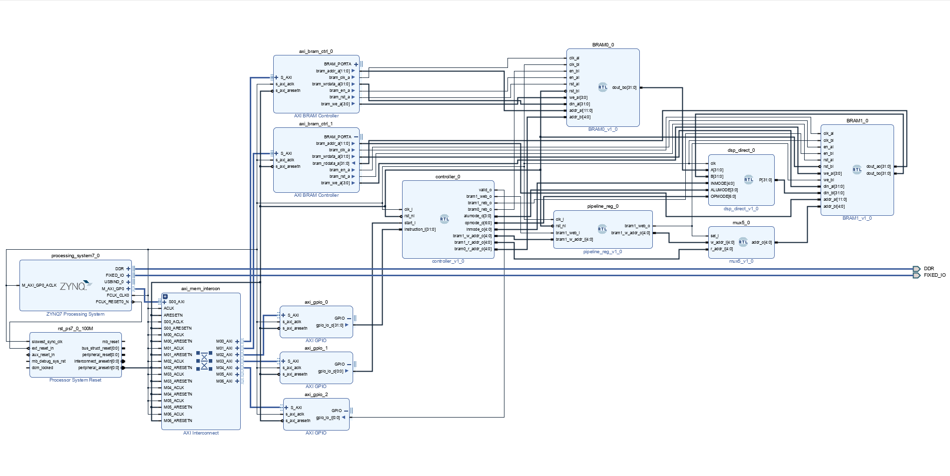
This project uses ZYNQ processor, block RAM, and DSP module to implement a simple computing system.
-
controller
-
Receiving
instructions_ifrom axi_gpio_0 andstart_ifrom axi_gpio_1 -
States
-
IDLE: resettingcounterto zero. Ifstart_ipulls high, going to stateDECODE -
DECODE:-
decoding the 32-bit inputs
instruction_iusing the following specification and outputting the decoded results31 30:27 26:20 19:15 14:10 9:5 4:0 bram1_web_o&bram1_eb_o&bram0_reb_oalumode_oopmode_oinmode_obram1_w_addr_obram1_r_addr_obram0_r_addr_o -
Going to state
EXECUTEstate
-
-
EXECUTE:- Using
counterto count the execution cycles of current instruction - Going to state
DONE
- Using
-
DONE- Pulling
valid_oto high - Going to state
IDLEwhilestart_iis low
- Pulling
-
-
-
pipeline_reg
- Using 3 levels pipeline registers to hold the value of
bram1_web_iandbram1_w_addr_i, which are connected to the outputs of controller
- Using 3 levels pipeline registers to hold the value of
-
mux5
-
inputs:
-
sel_i: connected tobram1_web_o[4:0]of pipeline_reg -
w_addr_i[4:0]: connected tobram1_w_addr_o[4:0]of pipeline_reg -
r_addr_i[4:0]: connected tobram1_r_addr_o[4:0]of controller
-
-
output:
addr_o[4:0]: connected toaddr_b[4:0]of BRAM1
-
Outputs
w_addr_i[4:0]ifsel_iis high, otherwise outputsr_addr_i[4:0]
-
-
BRAMs
-
BRAM0: written by CPU via Port A; read out by Controller via Port B and sent to Input A of DSP
-
BRAM1: Read and write by the CPU via Port A; read out the Input B sent to the DSP by the Controller via Port B, and write the operation result of the DSP
-
Specification of BRAMs:
BRAM0 BRAM1 Block Memory Size 32kb 32kb RAM mode TDP TDP READ_WIDTH_A 0 36 READ_WIDTH_B 36 36 WRITE_WIDTH_A 36 36 WRITE_WIDTH_B 0 36 WRITE_MODE_A WRITE_FIRST WRITE_FIRST WRITE_MODE_B WRITE_FIRST WRITE_FIRST
-
-
dsp_direct
-
Data input: A & B
-
Data output: P
-
Specification
Attribute Value AREG 1 BREG 1 PREG 1 ALUMODEREG 1 INMODEREG 1 OPMODEREG 1
-
Below are more detailed descriptions of the communication and behavior of PS and controller.
| PS | controller |
|---|---|
| Sends an instruction | In state IDLE |
| Sends a start signal | |
Receives the start signal from PS, then enters the decode state |
|
Decodes the instruction, then enters the EXECUTE state |
|
| Waits for DSP to finish the execution | |
Enters the DONE state, then sends a valid signal to PS |
|
| Receives the valid signal from controller | |
| Sends a clear signal | Returns to the IDLE state |
Question: How many DSP48E1 are on PYNQ-Z2?
Answer: 220

