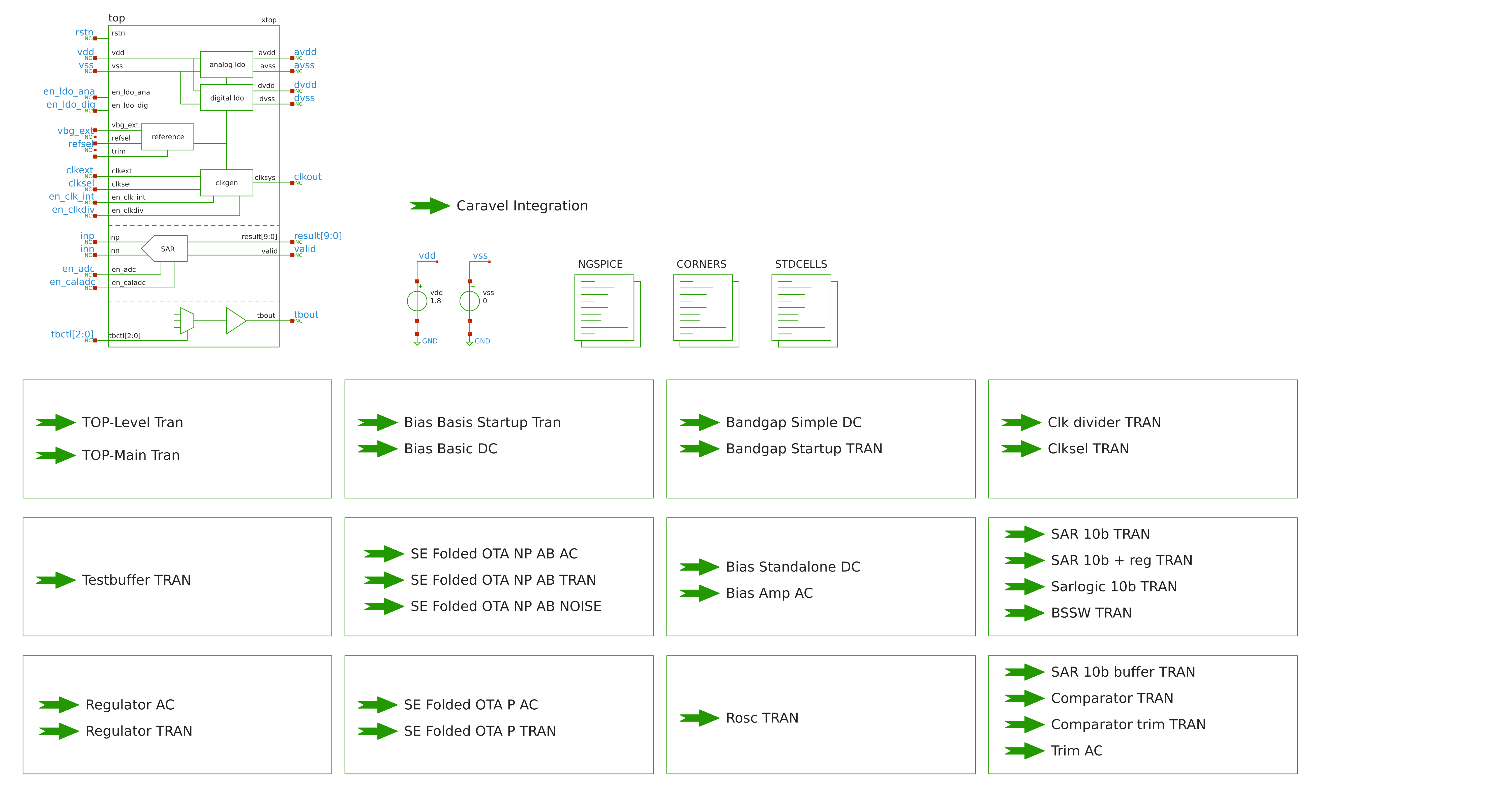
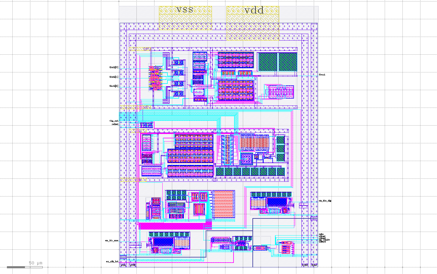
This submission features:
- Many detailed improvement to the previous mpw6 submission.
- Critical bugfixes related to connection issues on top-level.
Blocks in this submission:
- 10 bit SAR-ADC
- Bandgap reference.
- Testbuffer with multiplexer input.
- Clock generator
- 2 linear regulators, 1.2V and 1.5V.
- Bias current/voltage generator.
Included are:
- Hierachical GDS of the whole layout with all individual blocks.
- Schematics for all parts of the layout.
- Testbenches for all the individual blocks.
- Simulation corners setups for process corner simulations.
- FEM simulation setup for DAC capacitor.
- Verilog Code for SAR logic
Simply source cadrc in the xschem folder and execute xschem afterwards to get an full overview.
The layout was created using magic with the open_pdk sky130 setup as a pcell generator and klayout for the layout and assembly of the gds.
\
The ADC is a differential 10 bit SAR, with a capacitative DAC.
| Parameter | Min | Typ | Max | Unit |
|---|---|---|---|---|
| 1.8 | V | |||
| 1.8 | V | |||
|
|
V | |||
|
|
V | |||
|
|
V | |||
| Resolution | 10 | bits | ||
| 10 | MHz | |||
| -20 | 85 | °C | ||
| Area | 0.08745 | mm² | ||
| 3 | pF |
* 3.3V if ADC is not sampling the input signal.
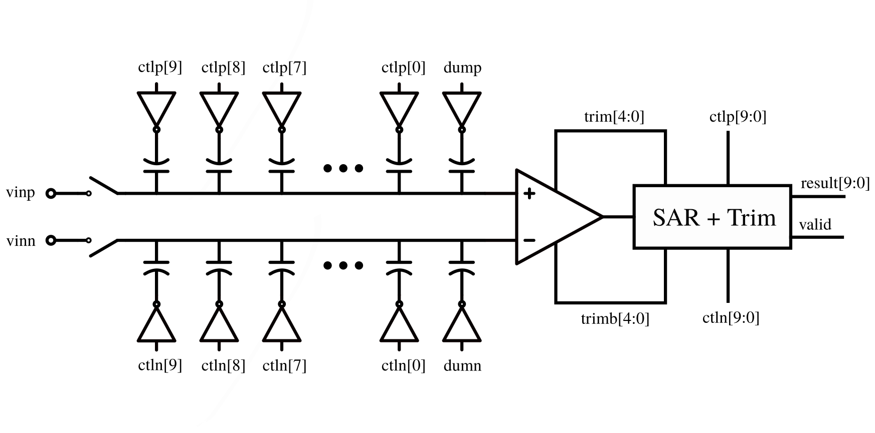
The Architecture of SAR is shown below. It is a differential architecture with a top-plate sampled CDAC.
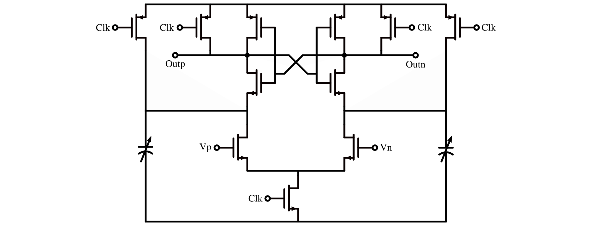
The comparator is pretty standard single stage topology. It features a trim array to calibrate its input offset.
The entire control logic is synthesized using the openlane flow. This allows to easily integrate the trim logic for the comparator into the overall control logic block.
For faster simulation the ngspice mixed-mode xspice feature was used. Yosys can be used to synthesize a xspice compatible netlist that only uses code-model components (NAND, NOT, DFF etc.) which speeds up simulation substantially.
The DAC is a capacitative DAC made from a total of 1024 unit caps per side.
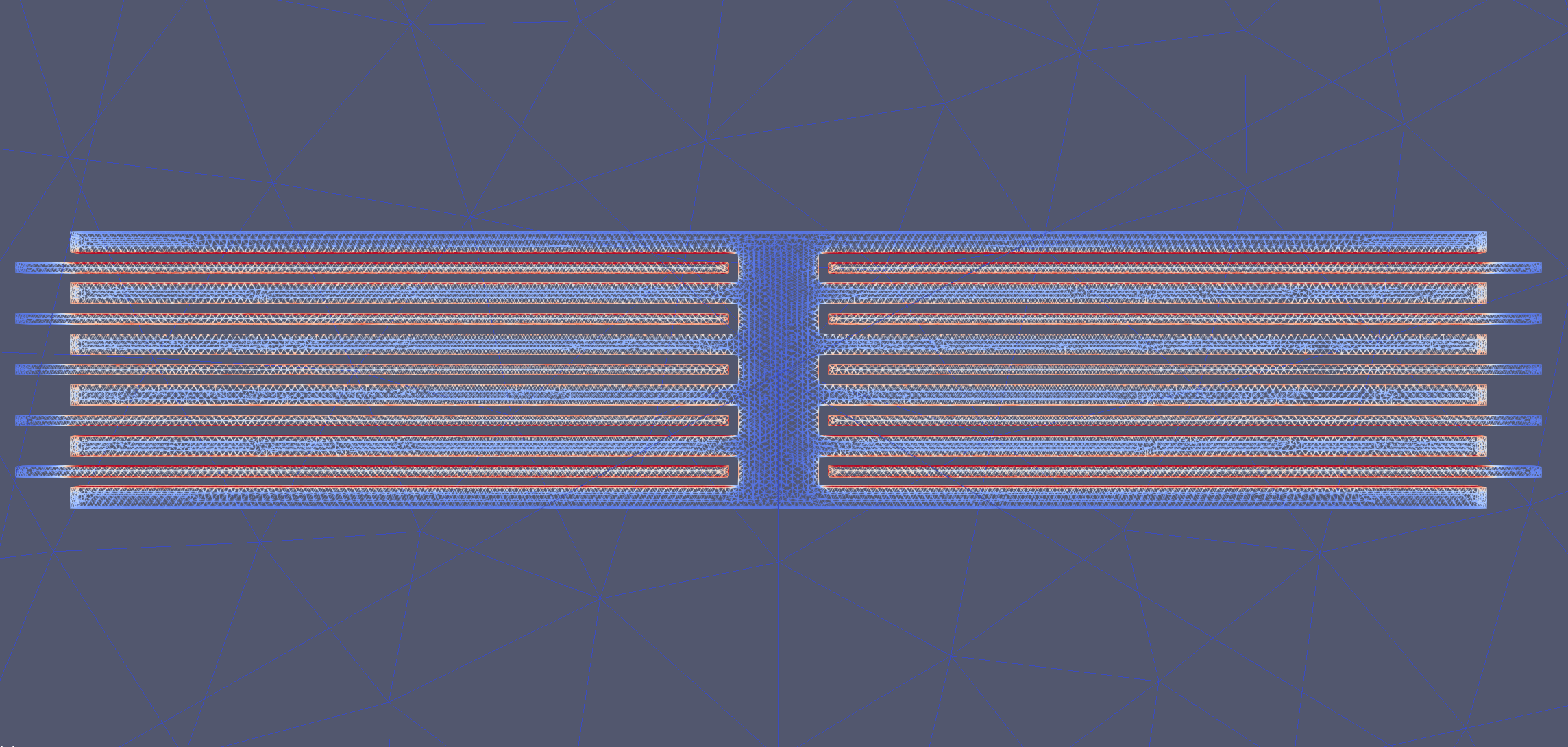
The unit size of the DAC elements is ~3fF based on FEM simulation carried out with Elmer FEM. You can find the full simulation setup in the elmer subfolder of this repo.
The process is:
- klayout with gds3xtrude to get a stl mesh of the layout
- freecad to convert mesh to step and encapsulate layout in boundary.
- gmsh to create a .msh 3D mesh from the step file.
- ElmerMesh to convert the .msh file to Elmer compatible mesh.
- ElmerGUI to define boundary conditions for the problem.
- ElmerSolver to solve for the electric field, capacitance etc.
- Paraview to verify the solution.
The DAC is top-plate sampled using a bootstrapped switch.
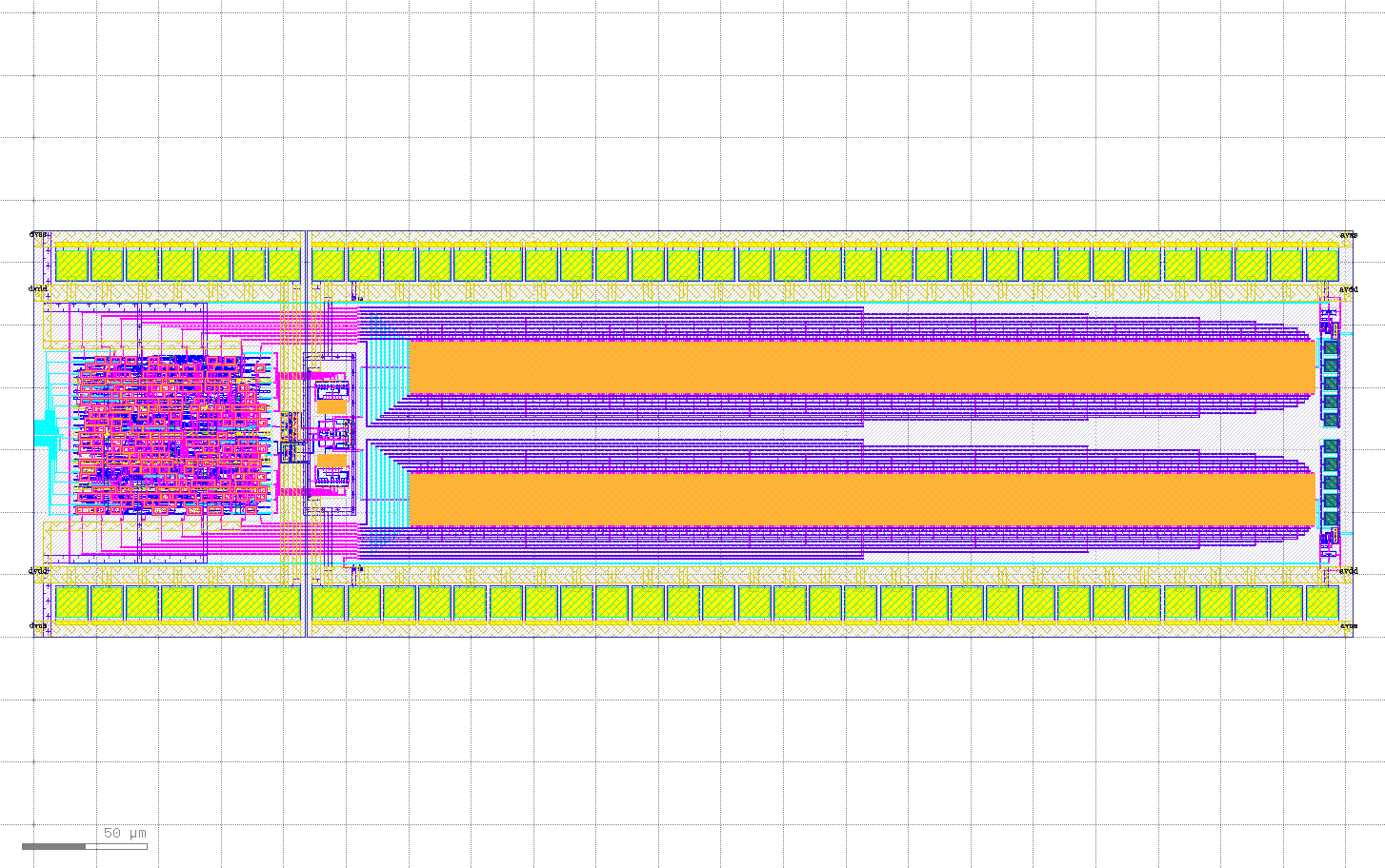
The complete SAR-ADC layout can be seen below. It occupies an area of approximately 0.08745 mm² (530 μm x 165 μm).
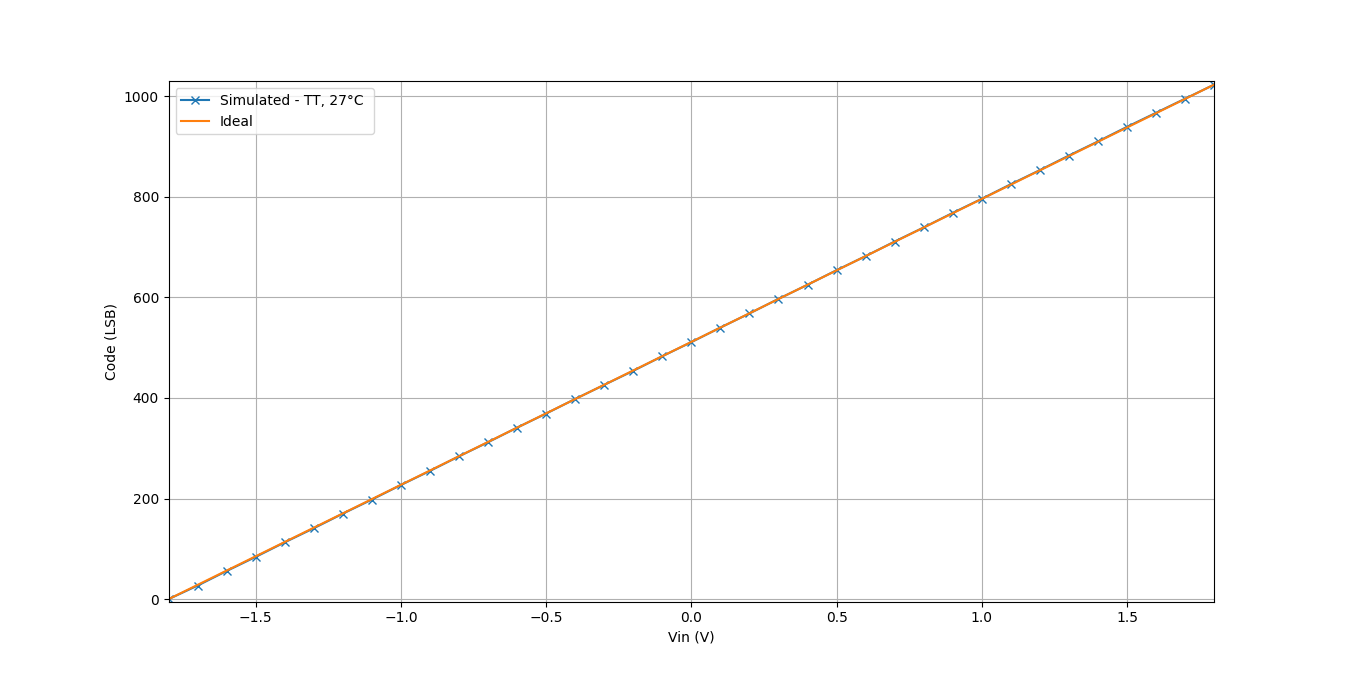
The result of a input voltage sweep across the full input range (-1.8V to 1.8V) can be seen below.
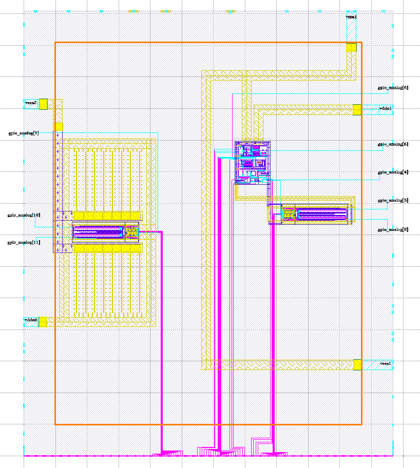
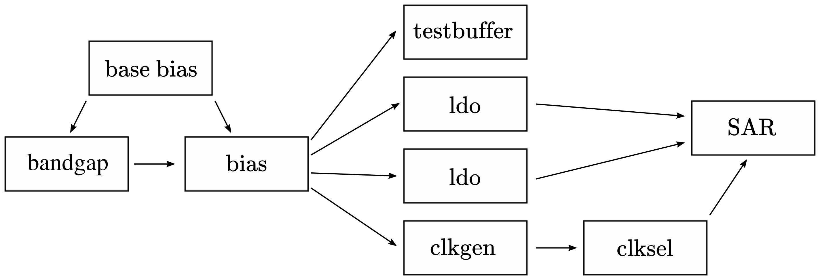
The main section contains various blocks that support the independent operation of the ADC.
The complete Main layout can be seen below. It occupies an area of approximately 0.1054 mm² ( 285 μm x 370 μm).
All parts have been simulated, using ngspice, for PVT where relevant.
- TT, SS, SF, FF, FS + Cmax, Cmin + Rmax, Rmin
- Voltage +-10%
- Temperature range -20° to 85°
To carry out PVT simulations, I used my custom ngsim python package that allows to manipulate spice netlists between runs.
A lot of different simulations were carried out on the individual blocks. The testbenches can be found in the xschem/tb folder under the respective block name.
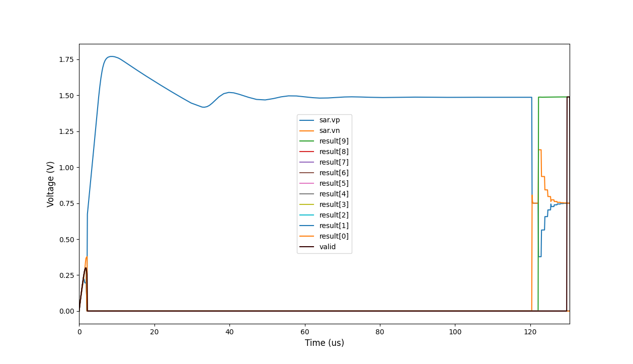
A complete extracted top-level simulation was carried out using a modified PDK and Xyce.
An example from system startup to completion of the first SAR conversion cycle with zero differential input voltage can be seen below.
It shows the output voltage of the positive and negative DAC side. This simulation utilizes all internal blocks, such a bandgap, ldo and oscillator to operate the ADC.
If this project gets a place on the MPW7 shuttle, I will continue to characterize the ASIC, using a opensource measurement flow. The results will then be published on this page/repo
Very detailed and good ressource on SAR-ADC design. A Low Power 10-bit SAR ADC in a 45nm process - V.A. Dyachenko
Various topics from bandgap reference to sampling switch circuits. A circuit for all Seasons - B. Razavi
- Connection to caravel wrapper on top-level
- Increased metal widths and vias.
- Improved regulator layout.
- Improved bandgap amplifier performance.
- Updated verilog of SAR, to keep valid pin in a high state after single shot conversion.
- Adressed potential antenna issue in DAC connection.
- Overall layout cleanup.
- Added sx-cut to allow for seperate ground extraction.
