TABLE OF CONTENTS
- WP3: Wilson's Pew-Pew Panels
- Software dependencies
- Designing the panels
- Building the panels
- Contributing and reporting issues
This project provides the instructions to create a custom design of A-RGB panels. The repository includes a python script (wp3_designer.py) that allows to design a custom composition of panels and then outputs several files to help manufacturing the panels. A parametric CAD file (that can be edited in FreeCAD) allows to quickly generate STL files with appropriate dimensions to 3D print the edges of the panels.
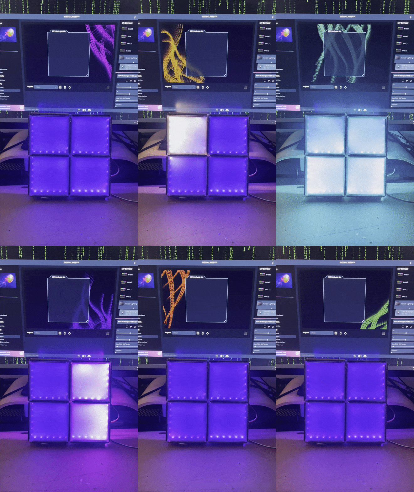
In my original vision, these panels are meant to be used with SignalRGB - which is why I included a special section dedicated to using them in the software. However, these panels are nothing but a fancy set of A-RGB strips: you can of course connect them to any hardware that is able to control NeoPixel/WS2812 LEDs!
| The question that probably nobody asked: why Wilson's Pew-Pew Panels? Well, Wilson is the name I gave to my PC while Pew-Pew is the sound that my girlfriend used to do to describe the lighting effects of my tower build. Hence, the name was born! 💻✨✨ |
|---|
| ℹ️ This software is used to export CAD files to be printed in 3D. If you are planning to create the supporting walls in a different way, e.g., using cardboard, you can skip this. |
|---|
Installing the program should be very easy: just head to the FreeCAD download page and download the installer. Launch it and install the software.
| ℹ️ this is an optional dependency that is required only if you run the script from its source. You can otherwise just run the "compiled" script (see the section Using the designer executable). |
|---|
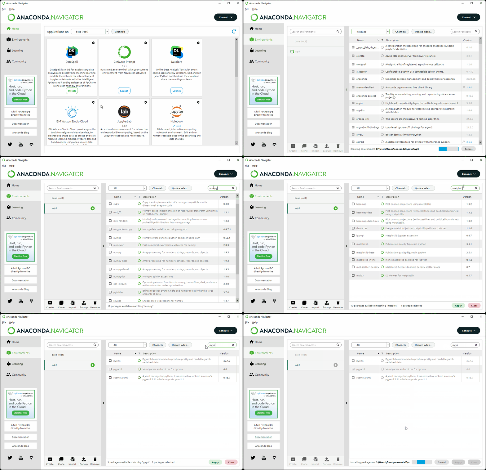
The wp3_designer.py script requires a valid Python installation with very few additional packages. If you know how to use Python already, just make sure that the packages Matplotlib, NumPy and PyYAML are installed and skip to the next section. If you do not know how to install Python, or you are not entirely sure, in the following there is a quick and simple way based on Anaconda. These steps have been tested in Windows, but they should be very similar under Ubuntu and MacOS. In addition, if you know how to use pip, you can do pretty much the same by pip installing the required packages from a terminal, without using Anaconda at all. As best practice, make sure to use venv or virtualenv to create a virtual environment to contain the packages and not mess with your local installation.
Anyway, here are the instructions to download all Python dependencies:
- Download the installer from the Anaconda Distribution page.
- Install Anaconda by following the wizard. The default options should be fine.
- Launch Anaconda Navigator and on the left select Environments.
- You should see a pre-installed environment, named base (root). In the bottom, you should be able to create a new environment by clicking on the create button (featuring a "+" icon).
- Give a name to the environment, e.g., wp3.
- Make sure that, next to the label Packages, Python is checked while R is unchecked. You should be able to select a Python version. I recommend using the same version as the one used by FreeCAD (
3.8.XXat the time of writing) since this allows to export STL files automatically, but do as you please. - Click on Create and wait for the environment to be ready.
- You should see a list of packages that are already installed. On the top, switch from the option Installed to All.
- On the top-right, there should be a package search bar. Click inside it and type
numpy. In the list, look for the package namednumpyand select it. Go back to the search bar and typematplotlib, then selectmatplotlibfrom the package list. Do the same a third time to locate and select the packagesruamel.yamlandselenium. - In the bottom right corner you should see a green button showing the text Apply: click on it. Anaconda will then open a pop-up window asking to install several packages. Click on Apply to install the three selected packages and their dependencies. This might take a while, just be patient and wait.
- Click on the green button with the "play" icon, next to the environment name.
- Select the option Open Terminal (it should be the first one).
- In the terminal, type
pip install webdriver-managerand press enter.
PyYAML instead of ruamel.yaml. Make sure to select the latter, not the former! |
|---|
Python is now configured! You can close the Anaconda navigator and proceed to the next step.
The design pipeline is quite simple: you firstly launch the script wp3_designer.py (or its executable equivalent, wp3_designer.exe), which allows to create a custom design for a set of panels. Once the design is ready, the script provides some information about the material to be purchased and few "instructions" to manufacture the panels. You then have to adapt the CAD files and export STL meshes for 3D printing.
To start the designer, you have two options:
- Using the "compiled" version of the script,
wp3_designer.exe. This is recommended if you are new to Python and/or not willing to install it. - Running the script itself from a terminal. This might be interesting if you plan to modify the script at some point.
Download the executable wp3_designer.exe, place it in a location of your choice and then double click on it. It will take a moment for the program to start, but that should be all!
If you wish to use an older version, check the releases page and download the executable from the corresponding assets.
If you already used Python before, this should sound very familiar. If you did not, I hope the procedure is clear and detailed enough to make it easy and painless. Anyway, here is what you need to do:
- Download the repository, if you haven't done that already. If you downloaded the source code using this link, make sure to extract the content of the archive in a location of your choice! You can also do it from the command line via
git clone git@github.com:francofusco/wp3.git(ssh) orgit clone https://github.com/francofusco/wp3.git(https). - Open Anaconda Navigator and on the left, select Environments.
- Select the environment that you previously created (see Python and Anaconda).
- Once it has been activated, click on the green button with the "play" icon, next to the environment name.
- Select the option Open Terminal (it should be the first one).
- A command prompt should open. Go to the location where you stored the source code using the
cdcommand followed by the path to the directory that contains it. The command might look likecd C:\Users\username\Documents\wp3. - Now type
python wp3_designer.py.
After launching the designer, a dialog window should open, asking to create a new project or load an existing one.
If you choose to create a new one, enter its name and change the default parameters if you wish (more details about their meaning are provided in the section Configuration of the designer). The project will be stored inside a folder with the given project name and a configuration file, named config.yaml will be created.
If you wish to load an existing project, move to the folder that contains it and select its config.yaml file.
This step is a "hidden one", in the sense that it is run silently right after creating or loading a project. If FreeCAD has been installed and the Python interpreter can locate it, then the designer will open the parametric CAD file cad/wp3-walls-v2.FCStd and update its parameters according to the project settings. It then exports STL files for walls and joints, so that they can be 3D printed.
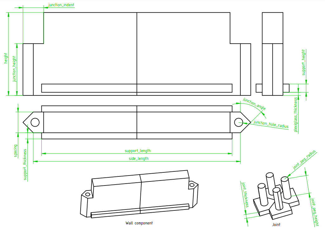
By default, the only parameters that are updated are the side length and spacing of panels. However, you can update other parameters as well. There are two ways to do it, the first being to directly modify cad/wp3-walls-v2.FCStd (I suggest that you make a backup copy first). Open the file in FreeCAD and in the list of components (the tree view on the left) double-click the spreadsheet named params. It should open the list of parameters used by the CAD project. The parameters colored in green are those that you would normally have to edit to adapt the design to your choices and export STLs manually. Red parameters are calculated from other values and should not be edited manually. The remaining parameters are "advanced ones". You are free to change them, but beware that large changes could break a design.
The second (preferred) way to change parameters in the design is to specify their values inside the config.yaml file. Please, refer to the corresponding section below, FreeCAD settings.
When working on a project, a window should open that looks like the following:
This is the design window, that allows you to create a custom composition of panels that you will later build. To change the composition, you can do the following:
- Click anywhere within the design space to add or remove a tile.
- Press
Ato remove all tiles,CTRL+Ato fill the space with as many tiles as possible. - Press the space bar to toggle all tiles.
Once you are satisfied with a design, just close the window.
The program will now start a routing step, in which it tries to determine a nice placement for the cables, so that you do not need an exaggerate amount of wire and the back of the panels does not become a tangled mess. In particular, the panels are designed so that a short LED strip can be glued in their inside and connectors can be soldered at the extremities of a strip to provide power and carry the signal. The connectors are positioned in one of the vertices of the polygonal shapes. To provide power and control all LEDs, it is necessary to connect all panels in sequence.
A very simple optimization algorithm has been developed to automate (at least partially) the routing process. Its task is to select, for each tile, one vertex where connectors are to be placed and then to choose the order in which tiles are visited. It will try to do so while keeping into account the following criteria:
- Two adjacent panels should not use the same vertex for their connectors;
- The order of visit should minimize the total travelled distance.
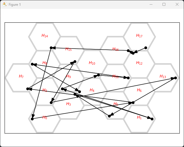
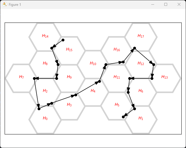
The routing process starts with a random path of wire from one panel to the other. This is generally a very bad solution:
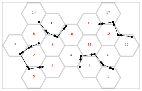
As you can see, the routing path is a mess here. Not only we jump all over the place, but some vertices feature multiple connectors. As an example, the tiles labelled H12 and H16 have their connectors in the same place, which is undesirable. A better path would be like the following:
To let the algorithm do its job, you can press the space bar. The current window will close and progress feedback will be shown in the active console. It takes a while, but the first run makes a huge difference. You can also interrupt the optimization at any time by pressing CTRL+C. After the routing has been optimized, it is shown again for validation. Do not expect incredible results: the algorithm is very simple and sometimes it struggles to find nice solutions. To overcome its limitation, you might have to repeat the process more than once (just hit the space bar again). Beware that sometimes the algorithm will not be able to improve the current routing. This does not necessarily mean that there is no better solution, but just that the optimization did not find one. Be patient, and try as many times as needed. Another way to make the problem easier is to let the algorithm break the routing path into multiple segments (this is explained later, in Routing settings):
Once you are satisfied with the obtained routing, you can close the window.
The program will now generate a couple of files that detail what components are needed and in which quantity to create the custom design. Most of the remaining steps rely on a list of available materials that you can specify in config.yaml, as detailed later in Materials settings. For now, you just need to know that there are two classes of materials used by the designer:
- Sheets are all materials that can be used to manufacture the fronts of the panels. As an example, I decided to use acrylic (which is transparent) to have a rigid surface and I glued an opaque film on top of it to better diffuse the light. Both materials can be purchased in sheets of given size and we need to cut tiles out of them.
- LEDs, organized in strips, are, well, LED strips. They come with a given amount of LEDs and density (LEDs per meter).
All materials have an associated cost, and one of the goals of the designer is to tell you how much of every material you need to buy to be able to create the panels while spending as little as possible.
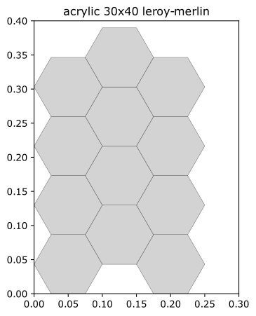
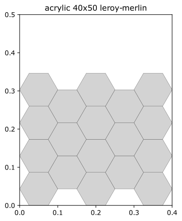
Each material that falls in the sheet category is characterized by a size. One of the jobs of the designer is to figure out how many tiles can be inserted in these sheets, and how. For each material, a pdf document is produced under the name design_info/tiling_<sheet-name>.pdf that shows how tiles can fit in the sheet.
As an example, there is a store near my house that sells acrylic sheets in a number of fixed sizes, such as 30x40cm2 and 40x50cm2. If my goal was to create the design shown in Choosing panel locations, which uses hexagonal panels with a side length of 5cm, this is how the two sheets would be filled:
Note that sheets do not always come in a predetermined size. Sometimes, they have a fixed width only, and you can buy as much material as you want, with the price increasing linearly with the chosen length. The designer is able to deal with this type of product as well, calculating the required amount of material in addition to finding how to fit tiles inside it.
Once all sheets have been processed in this way, it is time for the designer to figure out how much of every material should be bought. Once again, let's consider the design in Choosing panel locations, which includes 18 tiles in total. Using the two sheets above, there are two options: either buy two 30x40cm2 sheets or a single 40x50cm2 one. The choice, of course, depends on the cost. Even though the calculation is trivial, repeating it every time you change your design and making sure that you take into account all possible combinations can be error prone. For this reason, the designer does this job for you! Your only task is to specify which materials should be used, as described more in details in the section Assembly settings.
One further task of the designer is to choose how many LED strips should be purchased, which depends mainly on the size and amount of the tiles. Multiple LED strips might be available for purchase, with different lengths and LED densities. Similarly to what is done with sheets, the designer evaluates the appropriate amount of strips of each type to be purchased to satisfy the design requirements.
Let's clarify with an example, assuming the following specs:
- The design uses 18 triangular panels with a 8cm side
- We can purchase LED strips in the following varieties:
- 60 LEDs per meter, in two variants: 1m strips and 5m strips
- 30 LEDs per meter, in a single 1m variant
The problem is, how many 60-LEDs-per-meter strips should be buy, and which? And if we wanted to use 30-LEDs-per-meter strips instead?
Let's think about the first problem. The total perimeter of each tile is 24cm and you would therefore be able to fit at most 60 x 0.3 = 14.4 LEDs in each panel. Since a fraction of a LED cannot be put inside a panel, you will have to put 14 LEDs in each tile, corresponding to 14 / 60 = 0.233 meters of strip per tile. If you had to fill 18 panels, you would need a total of 4.2 meters of LEDs. There would be two purchase options then: either buy 5 1m strips or a single 5m one. Once again, the choice depends on the prices. And what about the 30-LEDs-per-meter strips? No need to perform calculations manually: the designer will once again do it for us.
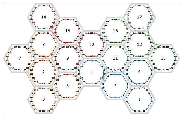
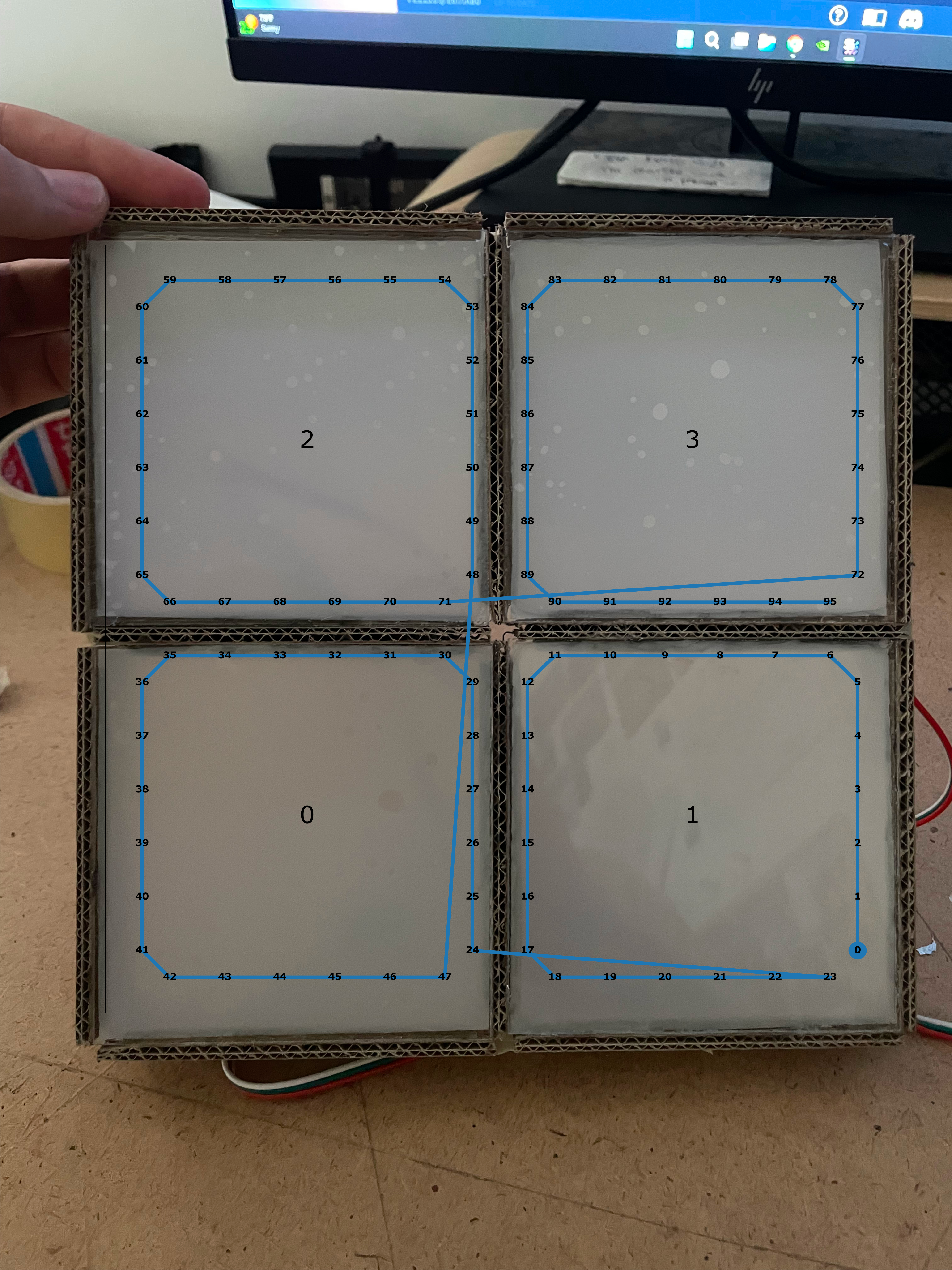
Another feature of the designer is that it is able to provide a detailed routing scheme to correctly address all LEDs in the design. In particular, given the optimal routing found before (see Routing), for each LED density in the available strips the designer will produce a scheme that looks like the following:
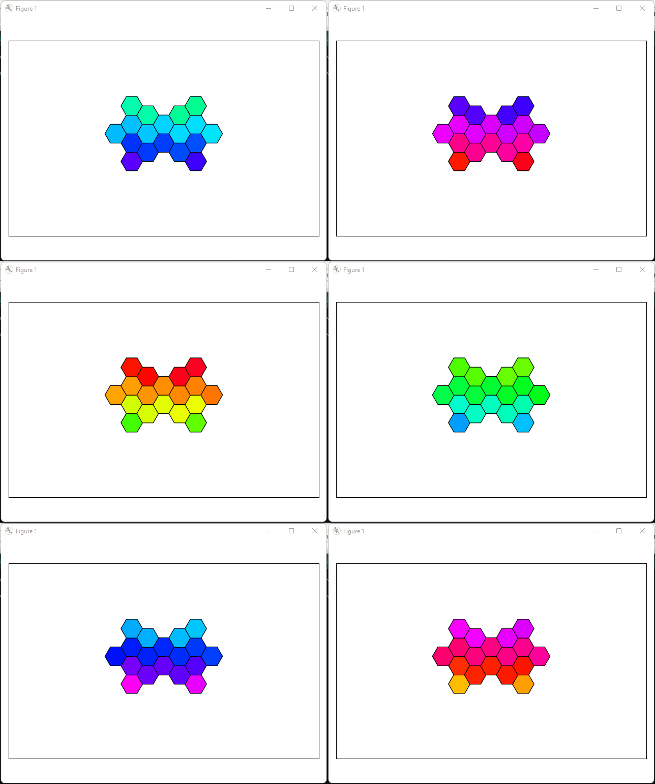
This scheme allows to locate each LED individually in the custom design. Furthermore, JSON files are produced that can be imported into SignalRGB to provide the necessary information to map each LED to a portion of the scene. Four components are generated: one that closely resembles the detailed routing scheme, one that puts all LEDs belonging to a tile in its center (in this way, each tile has a uniform color), one that represent a single tile with LEDs on its border and one that represents a single tile, with LEDs in its center.
For each given LED density, the routing scheme and the JSON files are generated respectively under the names design_info/wp3_routing_XXX_leds_per_tile.pdf and design_info/wp3_signal_rgb_PROJECT-NAME_XXX_leds[VARIANT].json, where XXX is the number of LEDs that the designer determined can fit in a single panel, PROJECT-NAME is, well, the name of the project and [VARIANT] is a string that depends on the type of exported component.
Last but not least, the designer configures and downloads from SRGBmods the firmware to be loaded on a Raspberry Pi Pico to use the panels in SignalRGB.
Last but not least, the designer produces a file, design_info/bill_of_materials.md, that summarizes the type and number of items that need to be purchased. It should include the following information:
- Number of parts that have to be 3D printed (with the list of parameters that have to be updated in the CAD).
- Calculate how many sheets of each kind should be purchased.
- Evaluate how many LED strips are to be purchased and estimate the required wattage (in a worst-case scenario).
- Count how many connectors are needed.
The designer can be customized by editing the YAML configuration file config.yaml present inside each project.
If you are unfamiliar with YAML, have a look at the Wikipedia page or just do a web search.
ℹ️ There is a bug in PyYAML related to scientific notation. If you want to write a number such as 0.01, you might want to write it as 1e-2. However, due to the bug you must include the decimal point in the base: 1.0e-2. |
|---|
Grouped under panels.
| Parameter | Type | Description |
|---|---|---|
rows |
int |
Number of rows in the designer area. |
columns |
int |
Number of columns in the designer area. |
spacing |
float |
Distance between the sides of two adjacent tiles, in meters. |
initial_tiling |
array |
Optional. This parameter allows to load a custom design on startup. The array is just a list of row-column pairs corresponding to tiles that should be visible on launch. After generating a composition of panels, the designer automatically updates the configuration file by storing the array corresponding to the current design. Therefore, you should not need to edit this parameter manually. |
In addition, tile specific parameters are grouped under panels/tiles.
| Parameter | Type | Description |
|---|---|---|
type |
str |
Type of each tile. It should correspond to the name of one of the Tile subclasses, e.g., Rectangle or Hexagon. |
variant |
int |
Optional. Allows to select a variant for the tile, if multiple variants are allowed. This affects the orientation of the tiles or how they stack together. |
Each tile type offers a couple of additional parameters that you can modify. These parameters might be specific to the selected Tile sub-class and not available for all types.
Grouped under freecad. All parameters are optional. If the values do not make sense, e.g., the height of a wall is smaller than that of the junction, errors might occur.
side_length, spacing, junction_angle and joint_num_walls. |
|---|
| Parameter | Type | Description |
|---|---|---|
freecad_path |
str |
Path to FreeCAD's bin directory, containing the Python module FreeCAD.pyd. |
plexiglass_thickness |
float |
Change the thickness of the plexiglass to the specified one. |
height |
float |
See technical drawing. |
support_height |
float |
See technical drawing. |
support_thickness |
float |
See technical drawing. |
support_play |
float |
See technical drawing. |
junction_height |
float |
See technical drawing. |
junction_indent |
float |
See technical drawing. |
junction_hole_radius_desired |
float |
See technical drawing. Note that the actual size of the junction hole radius could be smaller if there is not enough space. |
joint_thickness |
float |
See technical drawing. |
Grouped under routing.
| Parameter | Type | Description |
|---|---|---|
segments |
int |
Optional. Number of segments to be used in the routing procedure. Cannot be given if tiles_per_segment is specified. |
tiles_per_segment |
int |
Optional. Allows to use multiple segments in the routing, by specifying the maximum number of tiles to be traversed in each segment. Cannot be given if segments is specified. |
cache |
array |
Optional. This parameter allows to load on startup a routing that was found in a previous run, rather than starting from a random guess. The array contains two lists: the first one being the indices of the traversed tiles and the second one telling on which vertex of each tile a connector is placed. Every time a routing is determined, the designer updates the configuration file by storing the array corresponding to the current routing. Therefore, you should not need to edit this parameter manually. |
max_iterations |
int |
Optional. The routing algorithm works by generating random samples and trying to improve them. This parameter decides how many samples to generate in total. |
attemps_per_improvement |
int |
Optional. The routing algorithm works by generating random samples and trying to improve them by random mutations. This parameter decides how many unsuccessful mutations can be attempted before considering a random sample as improved. |
random_start_probability |
float |
Optional. When generating candidates for improvement, the algorithm will either create a random sample or select the current optimal solution and try again to improve it with more random mutations. This parameter provides the probability of generating random samples instead of selecting the current best. You should probably give it a value between 0.9 and 1.0. |
max_swap_distance |
int |
Optional. One of the possible mutations that is generated consist in swapping the order we visit two tiles. This parameter tells how farther the tiles can be. |
mixed_mutations |
int |
Optional. The algorithm performs mutations by selecting a tile and performing two distinct types of alterations: (1) swap its order of visit with all tiles within max_swap_distance and (2) change the vertex where its connector is located. In addition, a certain number of mixed mutations can be generated, in which both alterations are performed at the same time. Since the total amount of combinations is way too large for brute forcing, only a certain number of mixed mutations (controlled by this parameter) is selected. |
Grouped under signal_rgb.
| Parameter | Type | Description |
|---|---|---|
name_prefix |
str |
Optional. Prefix that should be used to identify the components inside SignalRGB. By default, the prefix is WP3 PROJECT-NAME. |
component_size |
int |
Optional. Maximum width and height of the component inserted in SignalRGB's canvas, when unscaled. This applies to the largest dimension, the smallest will be evaluated to maintain the correct aspect ratio. |
tile_size |
int |
Optional. Maximum width and height of the single-tile component inserted in SignalRGB's canvas, when unscaled. This applies to the largest dimension, the smallest will be evaluated to maintain the correct aspect ratio. |
Materials come in two types: sheets and LED strips. Each of them is grouped in a specific namespace, i.e., materials/leds and materials/sheets. In both cases, creating a new material requires to add a new namespace that is used as name for the material, and populate it with the required parameters. As an example, if you wish to add two LED strips named Adafruit NeoPixel and WS2812B strip found on Amazon, you can do it via:
materials:
  leds:
    Adafruit NeoPixel:
      number_of_leds: 60
      ...
    WS2812B strip found on Amazon:
      number_of_leds: 150
      ...
Grouped under materials/leds/strip_name. Each entry should have:
| Parameter | Type | Description |
|---|---|---|
number_of_leds |
int |
Number of LEDs in the strip. |
leds_per_meter |
int or float |
LEDs per meter in the strip. It might sound obvious, but if you know the length of the strip you can calculate the density as number of LEDs / length of the strip. |
watts |
float |
Optional. Power consumption of the strip. |
cost |
float |
Optional. Cost of the strip. |
url |
str |
Optional. Link to purchase the strip. |
Grouped under materials/sheets/sheet_name. Each entry should have:
| Parameter | Type | Description |
|---|---|---|
size |
[float, float] |
Width and height (length) of the sheet. If a sheet is sold with variable height (length), you can replace it with inf and the designer will select an appropriate size. As an example, size: [30.0e-2, 40.0e-2] specifies a sheet that is 30cm large and 40cm long, while size: [30.0e-2, inf] specifies a sheet that is 30cm large and with variable height (length). Do not pass inf as width, it will break the designer. |
cost |
float |
Optional. Cost of the sheet, either per unit (if both sizes are fixed) or per unit of length (if the height/length is inf). |
url |
str |
Optional. Link to purchase the sheet. |
In addition to the materials listed in config.yaml, the designer can read a list of materials from two additional sources:
- The file
materials.yamlstored in the online repository. - The local file
materials.yaml. This source is meant to be read during development.
The parameters under the namespace materials is just a list of available materials, but you also need to instruct the designer how to combine them. The way to do it is by adding a series of lists under of the namespaces assembly/leds and assembly/sheets. The elements of these lists should be material names declared before.
Assemblies are best explained via an example. Say that you found 4 kinds of strips:
strip 1has 30 LEDs and a density of 30 LEDs/m;strip 2has 60 LEDs and a density of 30 LEDs/m;strip 3has 60 LEDs and a density of 60 LEDs/m;strip 4has 300 LEDs and a density of 60 LEDs/m.
We can ask the designer to evaluate how many strips would be needed if we wanted our LED density to be 30 LEDs/m by adding the array ["strip 1", "strip 2"] as an entry in assembly/leds:
assembly:
  leds:
    - ["strip 1", "strip 2"]
However, we might want to use strips with 60 LEDs/m instead. In this case, just add the entry ["strip 3", "strip 4"] as well, in a new line:
assembly:
  leds:
    - ["strip 1", "strip 2"]
    - ["strip 3", "strip 4"]
The designer will produce the files for both alternatives and it will be your choice which one to use.
Another use case of assemblies is when multiple materials are needed to manufacture a component. As an example, I decided to create the tiles using transparent plexiglass covered with a semi-opaque film. In this case, I need the designer to tell me how many plexiglass panels to buy, but also how long the opaque film should be to cover the whole surface. My configuration therefore looks like the following:
assembly:
  sheets:
    - ["acrylic 1", "acrylic 2"]
    - ["opaque film"]
The first list has multiple items because plexiglass can be purchased in sheets of different, but fixed, sizes. The second list has only one item since the film is sold with variable length and I want the designer to just tell me how much of it I need.
In addition to the LED strips and the sheets to manufacture the panels, you will need a couple more materials:
-
A bunch of JST SM 3 Pin Connectors, such as these ones. You will need two pairs of cables per panel.
-
A Raspberry Pi Pico to control the panels using SignalRGB.
-
A Power Supply Unit such as this one or similar, just make sure to choose the correct wattage! In alternative, you can borrow some power from the PSU of your PC, but make sure you will not draw too much current.
-
Electrical wire and connectors, to connect the panels to the microcontroller and to the PSU.
-
Soldering equipment.
-
A level shifter to make sure that 3V3 signals from the Pico are raised to 5V, i.e., the logic level used by the strips.
-
Not required, but recommended: screw terminals. They make it much easier to connect components to each others.
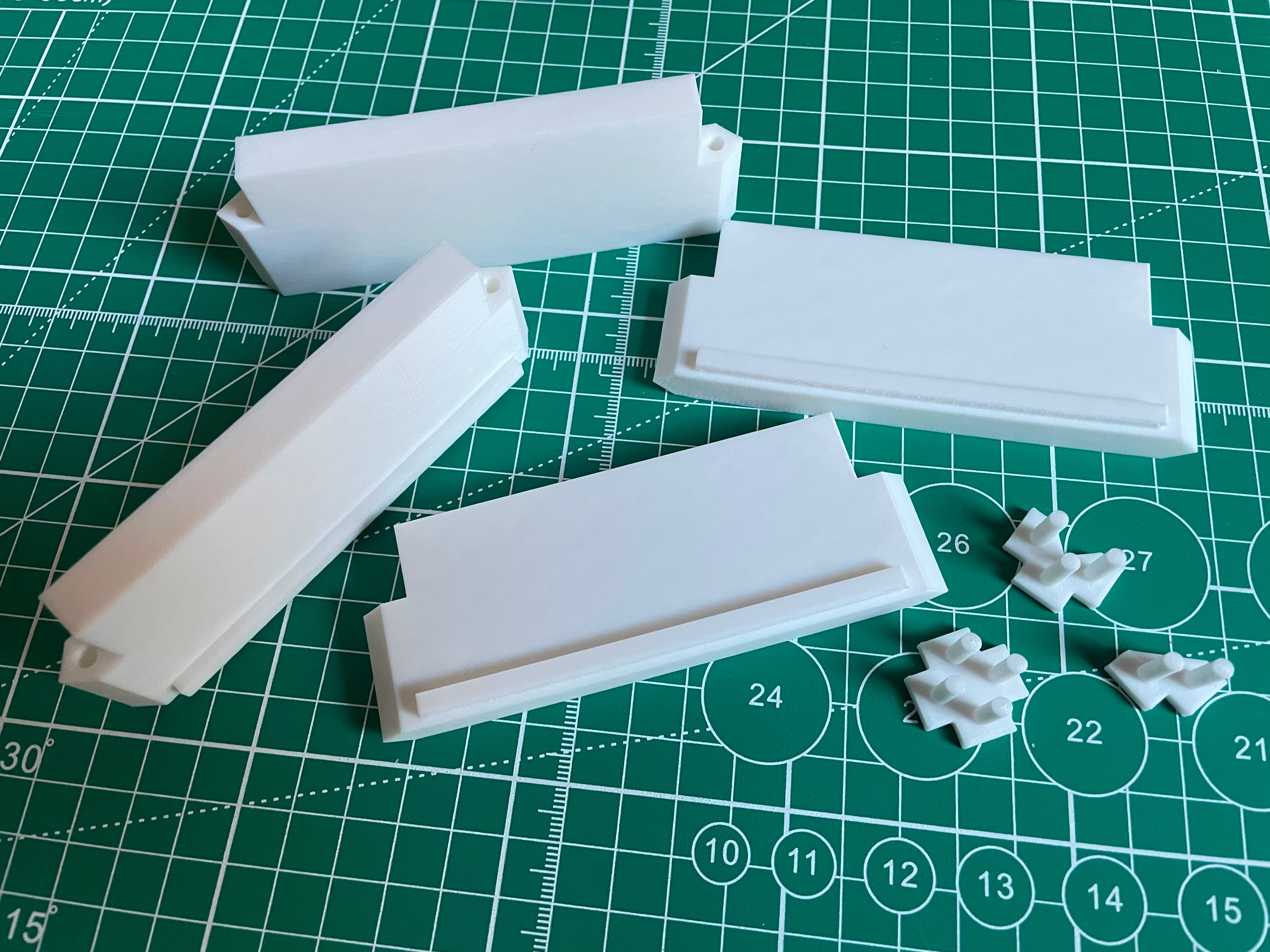
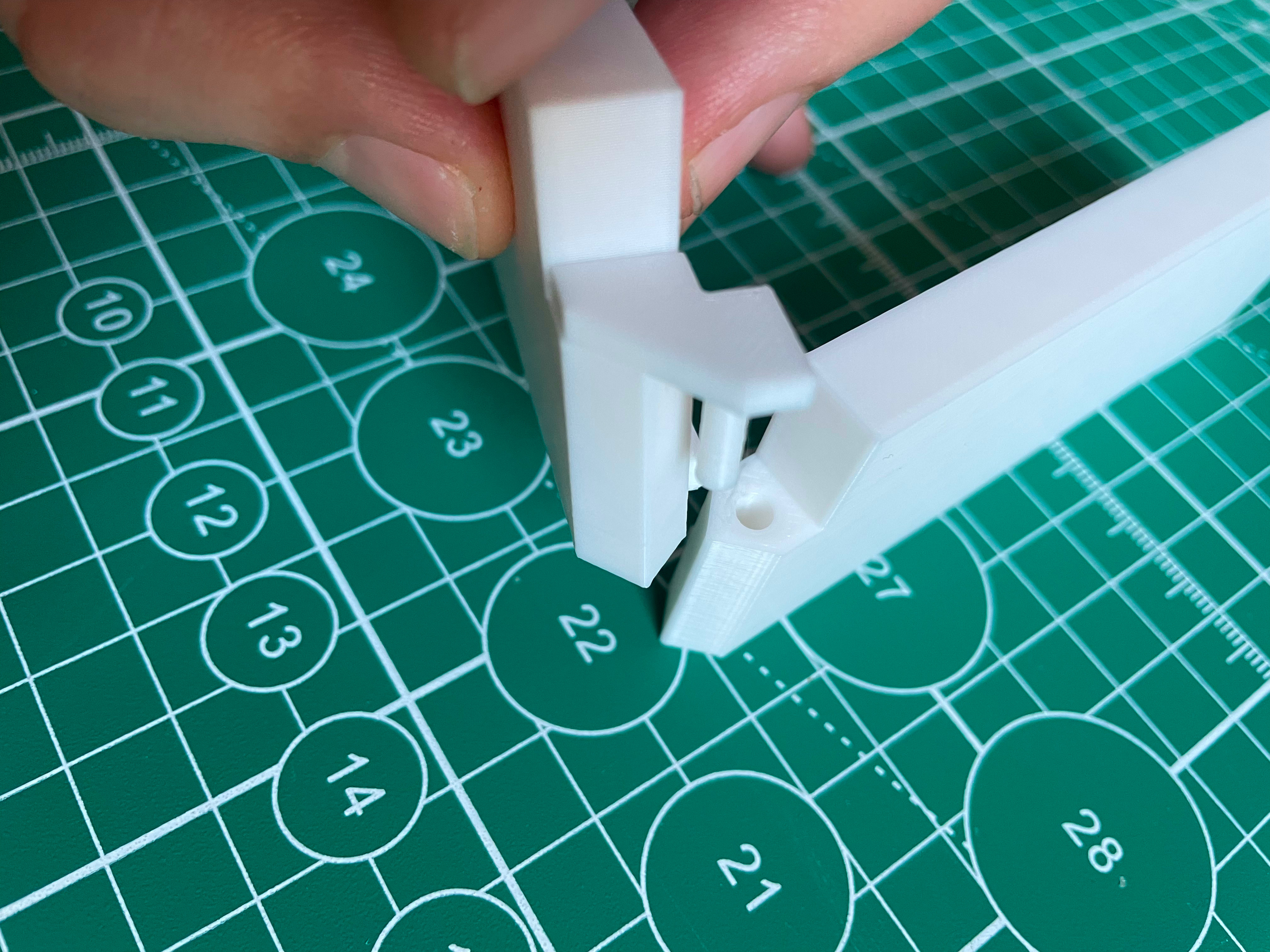
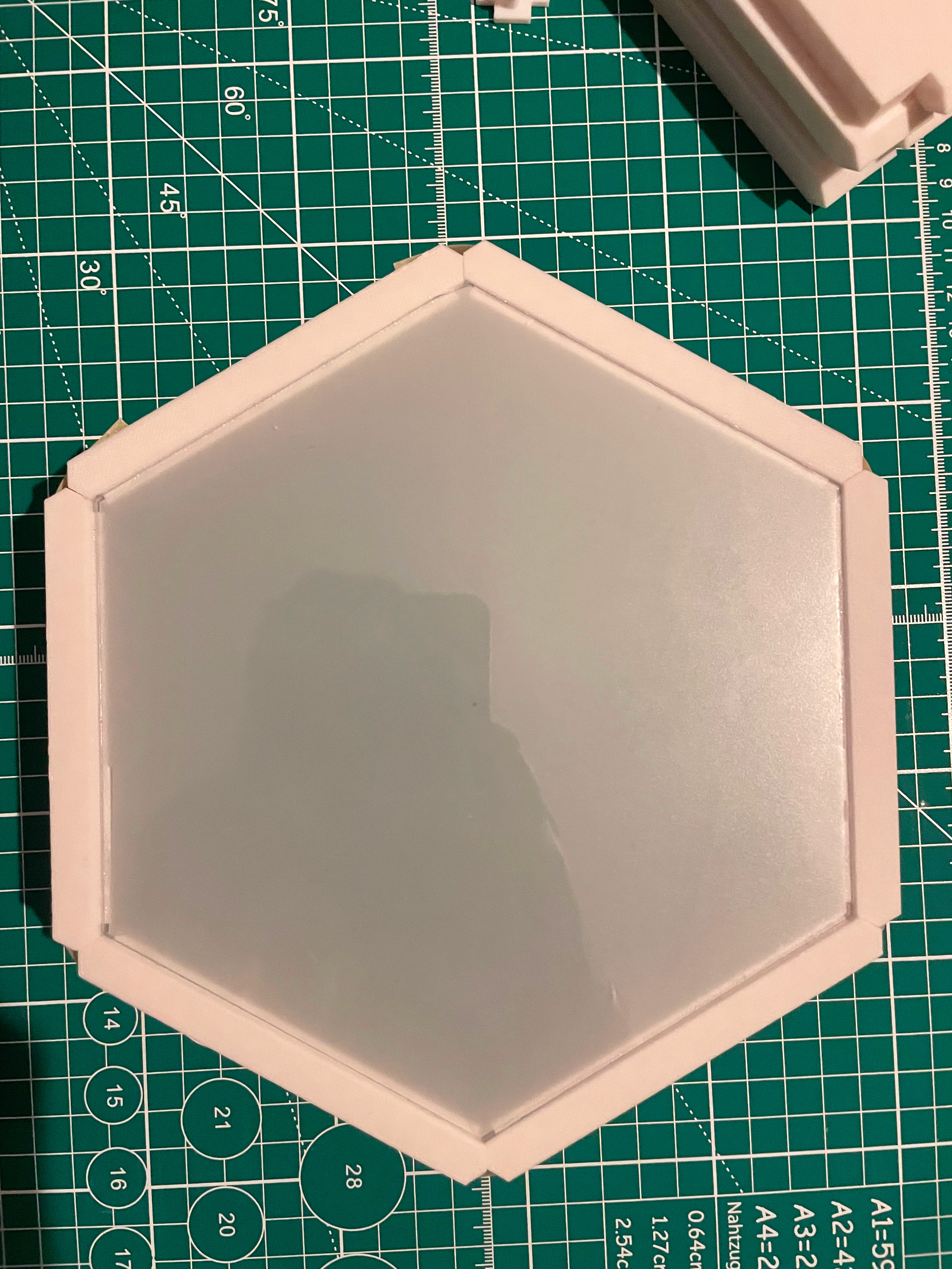
If you installed and configured FreeCAD, the designer should have exported some STL files that are ready to be sliced and printed. There are two types of component to be printed, walls and joints. Walls are further divided in inner walls (sides shared by two panels) and outer walls (sides belonging to a unique hexagon). The difference is that inner walls have a small support for the acrylic panels on both sides, while outer walls have this support on one side only. There are also different types of joints, each allowing to join a different amount of walls together. To know how many copies of each STL you have to print, look inside the bill of materials.
I will not give specific instructions to print these components, since I think this heavily depends on the printer you are using. Just as a guideline, in my case I simply imported the components in Cura to slice them, saved the g-code in a SD card and finally printed them with an Ender-3.
If 3D printing is not an option, a cheap and relatively quick alternative is to use cardboard to create the walls. This was the solution for my first prototypes. I completely disregarded aesthetics, but I believe that with a little more efforts one could easily achieve a nice result even with this material.
Just for reference, this is how I created the cardboard walls:
- I cut a set of 10x3cm2 rectangles which were used as walls.
- I cut small stripes to create the panel supports.
- I glued the stripes onto the walls where needed: on one side for outer walls and on both sides for inner walls.
- I marked all corners with a number (to make it easier joining them later) and cut away a small portion of cardboard in the vertices where the connectors were supposed to be located.
In my case, the easiest and cheapest way to create the panels was to use transparent acrylic and then apply an opaque film on top of it. Of course, other solutions are possible! Anyway, here is the process I followed:
- Using a cutter knife, cut the tiles out of the acrylic.
- Repeat the process using the opaque film, making sure that each film piece fits inside an acrylic tile with a little bit of margin.
- For each tile, remove the protective film from the acrylic and stick the opaque film on top of it.
- If using the printed parts, you can join walls together using the printed joints (you can add glue as well for increased rigidity) and then glue the panels to the structure. If you opted for other materials, attach walls and panels in the best way you can.
- Prepare the LEDs: cut them in strips with the required amount of LEDs and solder a pair of connectors at each end. Make sure to be consistent with the direction of the data pins and the connector types at each end, so that strips can be joined in series!
- Attach the stripes inside each panel. Make sure to respect the detailed routing diagram for a flawless integration inside SignalRGB 😉
To use the panels in SignalRGB, you can use a Raspberry Pi Pico and the amazing SRGBmods Pico LED Controller by FeuerSturm. All you need to do is to follow the setup instructions: click on the Display instructions about setting up Arduino IDE, in the bottom, and configure the Pico. In the last steps, when it tells you to open the file that you downloaded from SRGBmods, open instead the .ino sketch that has been downloaded in your project folder and use that one to program the Pico. Just for clarity, the firmware is generated by the designer by accessing the SRGBmods page, assigning channels and LEDs to pins, and by "clicking" on the download button.
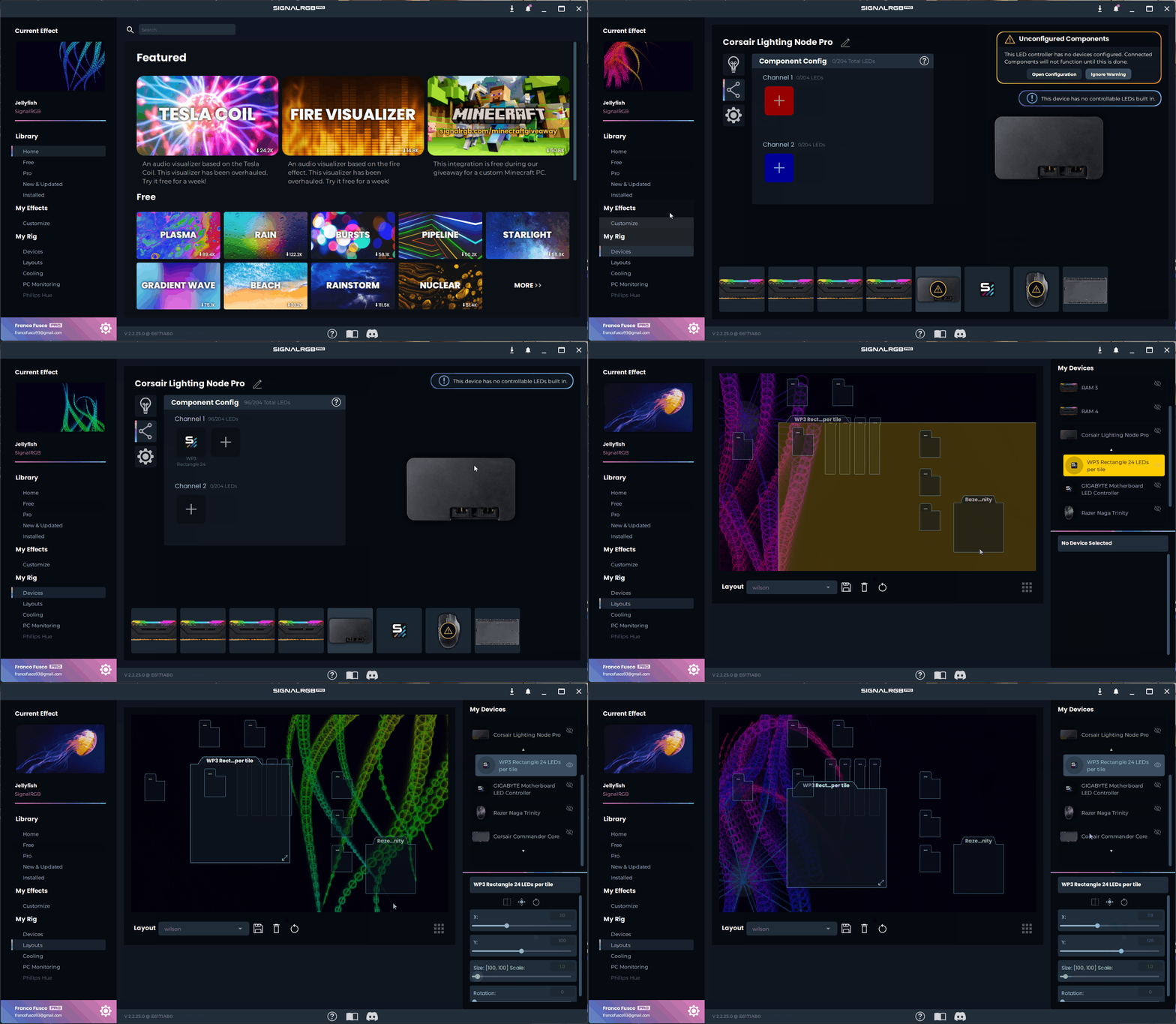
Depending on which LED density you decided to use, copy the corresponding json files into the directory Documents\WhirlwindFX\Components and restart SignalRGB. In the Devices page, click on the controller that you are using and click on the "+" button to add a component. In the brand filter, scroll down and look for WP3, then select the appropriate component. Go to the Layouts page and position the panels in the canvas. You are all set 🥳
If you happen to find a problem with the designer, do not hesitate to reach to me. The best way to do so is to open an issue describing the problem. Try to describe the problem you are facing, and perhaps include your config.yaml, as well as the log file .wp3_last_run.log that is generated after each time you run the designer.
| 🚧 👷 This section is to be written. |
For the moment, I will just keep a short list of things that will be worth mentioning:
- To create the executable you will need to download the PyInstaller package, e.g.,
pip install pyinstallerorconda install pyinstaller. Once that is done, you can run (in an Anaconda terminal) thebuild_exe.batscript to create an executable under Windows. - While log files are generated automatically, you can also change verbosity level from the command line. Type
python wp3_designer.py --helpfor the list of arguments that you can pass. - Code formatting:
- The style is the one enforced by Black. To keep the code formatted, include the package to your virtual environment (
pip install blackorconda install black) and run it from the top-level directory of the project:black .orpython -m black .. - You also need to check comments manually using the script
comment_checker.py:- Run
python comment_checker.py . wp3: it will scan all python files and tell you which ones contain comments that are too long, and at which lines. - Edit the flagged comments. This is a manual process, unluckily... To speed up the process, you can add the option
--annotatewhen runningcomment_checker.py. This overwrite the files by adding the marker<<<<<at the end of long comment lines. In this way, you can open the files and do a search for<<<<<to quickly find lines that need fixing.
- Run
- Whenever the code is pushed, a GitHub action will check formatting and report failure if either Black or
comment_checker.pyfind any issue.
- The style is the one enforced by Black. To keep the code formatted, include the package to your virtual environment (
- To add new panel types:
- Create a new python file inside
wp3/tilesand give it a meaningful name, e.g.,star.pyif you are creating star-shaped panels. - Create inside it a class that inherits from
Tileand implement the methodsconfigure(),configurable_parameters(),calculate_center(),create_patches(),vertices(),contains(),adjacent()and, optionally,get_variants()andexport_stl(). - Import the tile type into the
wp3/tilessub-module. The instruction (to be added intowp3/tiles/__init__.py) might look likefrom .start import Star.
- Create a new python file inside

