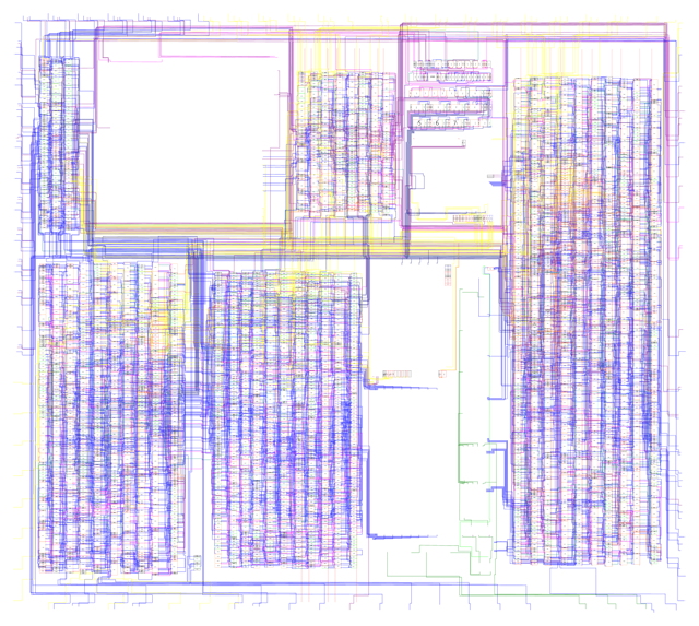
This repo contains an annotated overlay for the Nintendo Game Boy DMG-CPU-B chip die and the extracted schematics.
This was done manually with only a few automated checks so THERE'S A HIGH RISK OF ERROR. I'm in no way responsible if you made someone's life depend on this and it fucked up.
- All APU logic.
- All PPU logic.
- All I/O and timer logic.
- All DMA logic.
- All interrupt logic.
- Various stuff used for testing/debugging.
- CPU. Why: it's a standalone core which doesn't use the standard cell topology. Visibility isn't good enough and it's too complex for me, sorry.
- Clock complements. Why: They don't affect functionality. Only required because the DFF cells need a clock and its complement to work.
- Some analog parts. Why: Poor visibility, lazyness.
- Some cell groups related to embedded ROM and RAM blocks. Why: They don't affect functionality.
Just read the schematics :)
If you want to use the overlay:
- Get Inkscape
- Download the die picture from Digshadow
- Resize it to 8000px wide if you're using Inkscape 0.92.2, otherwise it may freeze
- Download the SVG overlay
- Open the overlay in Inkscape, import the die picture (chose link, not embed), stick it under the overlay layers, align it and lock it in place
- Have "fun"
Nets named FROM_CPU* and TO_CPU are connected to the CPU core but are not clearly identified. Many of them are trigger and acknowledge signals for interrupts. Others might be state indicators like the Z80 /M1 or HALT.
Some DFF clock polarities have to be verified.
The parallel-in-serial-out shift registers used for the serial link and video rendering are made of chains of set-reset-capable DFFs. Their loading logic require a lot of cells and seem complex, but in the end it forms something quite simple.
Rather than using multiplexers, many internal busses are instead tri-state capable. The "TRIBUFFER" cells are extensively used for this.
- Bit 4 and 5 of FF26 (NR52) can be written to.
- Bit 4 sets NET03 (APU test mode ?).
- Bit 5 allows software clocking of the CH1 sweep timer when NET03 is high.
- Bit 0 of FF23 (NR44) can be read. It relates to the CH4 prescaler.
- The current wave RAM address can be read in bits 4~0 of FF1C (NR32) when NET03 is high.
- The whole chip can be made a slave for an external CPU by using the test pins. This was already discovered by @Gekkio and maybe others.
- Probably other things I missed...
- Why ?
It is well known by emulator authors that the Game Boy is full of quirks. Knowing exactly how and when signals change can help reaching perfect accuracy.
- Why are the schematics not in an editable format ?
Because I used proprietary CAD software for speed and I didn't finish making the converter for the KiCAD format. I hope to be able to do that soon.
- What's up with the cell labels ?
They're random, unique names. The first letter corresponds to the column they're in on the silicon die.
- Many small lines aren't traced, why ?
I didn't bother tracing branching lines when their end point was near enough to see it on my 15" screen at the zoom level I used. They're reported on the schematic, of course.
- Why are there copies of logic blocks providing identical functions ?
It's a way to trade off die space for speed, it seems weird but it's useful. Look up "logic duplication".
- I found a mistake, how can I report it ?
Until I get the files exported in KiCAD format, please open an issue and describe what's wrong (cell name, net name, position on die, ...).
- How did you know which cells did what ?
I had to take guesses. Inputs and outputs are easily identified and the cell size gives some clues. When connections are made on the schematic, it becomes quickly obvious when a guess is wrong. Check out the cell zoo.
- How long did it take ?
Identifying the cells, isolating them, tracing the connections and the schematics took 191 hours.
If you find it worth it, I accept donations through Paypal: paypal.me/furrtek
Thanks to Gekkio, Tanjent and Kevin Murphy for the help.
