-
Download installer:
Xilinx_Unified_2021.1_0610_2318_Lin64.bin -
Run installer and then download a local network drive image
This makes it easier to install on multiple PCs later...
-
For Ubuntu 20.04, before running
./xsetup, first do the following:sudo ln -s /lib/x86_64-linux-gnu/libtinfo.so.6 /lib/x86_64-linux-gnu/libtinfo.so.5If you don't do this, the installer will fail at a later stage.
-
run
./xsetup -
Install Vitis: this includes Vivado!
-
Install PetaLinux
The KV260 board uses a quad FTDI FT4232HL chip, which is connected to the following:
- JTAG interface of the FPGA
- SOM UART
- STDP4320 UART
- MIO I2C M24C64 EEPROM WC_B write control
lsusb shows the following vendor id and product ID:
Bus 001 Device 014: ID 0403:6011 Future Technology Devices International, Ltd FT4232H Quad HS USB-UART/FIFO IC
The UART part should just work without driver (at least it did for me), but you need to install the udev rules file
to enable JTAG control:
cd ~/tools/Xilinx/Vitis/2021.1/data/xicom/cable_drivers/lin64/install_script/install_drivers
sudo ./install_drivers
result:
INFO: Installing cable drivers.
INFO: Script name = ./install_drivers
INFO: HostName = zen
INFO: Current working dir = /home/tom/tools/Xilinx/Vitis/2021.1/data/xicom/cable_drivers/lin64/install_script/install_drivers
INFO: Kernel version = 5.8.0-59-generic.
INFO: Arch = x86_64.
Successfully installed Digilent Cable Drivers
--File /etc/udev/rules.d/52-xilinx-ftdi-usb.rules does not exist.
--File version of /etc/udev/rules.d/52-xilinx-ftdi-usb.rules = 0000.
--Updating rules file.
--File /etc/udev/rules.d/52-xilinx-pcusb.rules does not exist.
--File version of /etc/udev/rules.d/52-xilinx-pcusb.rules = 0000.
--Updating rules file.

INFO: Digilent Return code = 0
INFO: Xilinx Return code = 0
INFO: Xilinx FTDI Return code = 0
INFO: Return code = 0
INFO: Driver installation successful.
CRITICAL WARNING: Cable(s) on the system must be unplugged then plugged back in order for the driver scripts to update the cables.
See also Xilinx installation manual.
As always, I had to reboot to make things stick after this...
- PROGRAM AND DEBUG
- Open Hardware Manager
- Open Target
- Auto Connect
Result:

Features:
-
FPGA part name: XCK26-SFVC784-2LV-C
- Not directly supported in Vivado. Need to select a board instead of a part...
- Close cousin of ZU5EV, however, when looking at the ZU5EV pinout, and compare it against the XCK26, there seem to be differences. E.g. the ZU5EV has much more pins in bank 66.
-
4x Cortex A53 @ 1.5GHz
- 256KB onchip memory, 1MB L2 cache
-
2x Cortex R5F @ 600MHz
- 128KB TCM per CPU
-
Mali-400 MP2 @ 667MHz
-
Video Codec Unit
-
256K logic cells
-
144 Block RAM blocks
-
64 UltraRAM blocks
-
1248 DSP slices
Documents
-
Kria SOM Carrier Card - Design Guide
- How to design a board that uses a Kria SOM.
- Figure 1 is important because it shows which SOM pins are going where.
-
- Quite a bit of overlap with the SOM Carrier Card Design Guide.
-
Kria KV260 Vision AI Starter Kit DataSheet
- Low of useful info.
-
Kria KV260 Vision AI Starter Kit User Guide
- Describes connectors, boot devices and firmware, getting started info, tools integration overview, board reset and firmware update/recovery.
-
Download petalinux image from this getting started link, not from this one.
-
Once the initial getting started is up and running, then use the command line options of the github smartcamera page.
- E.g. try with different resolution, try with rtsp -> VLC
-
kv260_pinout.pyis a Python dict will all information gathered.pin_process.pywill use the pinout file to create all kinds of tables etc.
-
Based on schematic: I went through all the SOM240_1 pins and derived their meaning.
-
The som240 board file contains useful interface signal naming.
-
k26c part0_pins.xml contains connector signal pin to FPGA pin mapping for some signals.
-
The project XDC files also contains some pin to signal mappings.
M2C: module to carrier board C2M: carrier board to module
- IAS0 connector: OnSemi image access system (IAS) camera module interfacesupporting four MIPI lanes. Connects to OnSemi AP1302 ISP device sensor 0 interface.
- IAS1 connector: OnSemi IAS camera module interface supporting four MIPI lanes.
- JTAG: when FTDI chip has
LS_OE_Bpin asserted then JTAG pins are driven. Otherwise, the JTAG connector can take over.
-
Derived from Vivado project (kv260_ispMipiRx_DP)
-
Zynq UltraScale IP Block Clock Configuration: Input Clocks:
- PSS_REF_CLK: 33.33MHz (generated on the SOM itself?)
- SATA: Ref Clk2: 125MHz
- Display Port: Ref Clk0: 27MHz
- USB0: Ref Clk1: 26MHz
- These Ref Clk speeds match the speeds of the clockgen in the KV260 schematic
Output Clocks:
- PL Fabric Clocks: PL0 to PL1 all set to 100MHz.
-
Block Design:
- PL0 clock -> Clocking Wizard IP block -> 5 clocks: clk200M, clk100M, clk300M, clk50M, clk600M
All of this below assumes that you have PetaLinux running on the KV260 board. In other words, you went through the Getting Started sequences to create an SDCard with PetaLinux and booted the board from that.
Once that's done, the PS of the FPGA is configured such that there's 100MHz clock for the PL, and the PL part is switched on and ready to receive a bitstream, from the PS or through JTAG.
On the KV260, I can find no clock that can be used straight by the PL part, so the PL part must get its clock from the PS. And this needs a whole song and dance with the IP Block GUI to link your own design to the clock of the MPSoC part.
That's what described below.
It's possible to have the SoC run a barebones firmware instead of Linux, but I haven't gotten this far yet...
Another thing to keep in mind is that I'm using the FPGA IO pins that I figured out along the way
(and that can be found in ./kv260_pinout.py.) I'm not using defintions from the board files,
because I haven't figured out how to do that yet...
-
Start Vivado
-
Quick Start -> Create Project
-
Project name:
kv260_fan_test, Project location:/home/tom/projects -
Project Type: RTL Project

-
Default Part
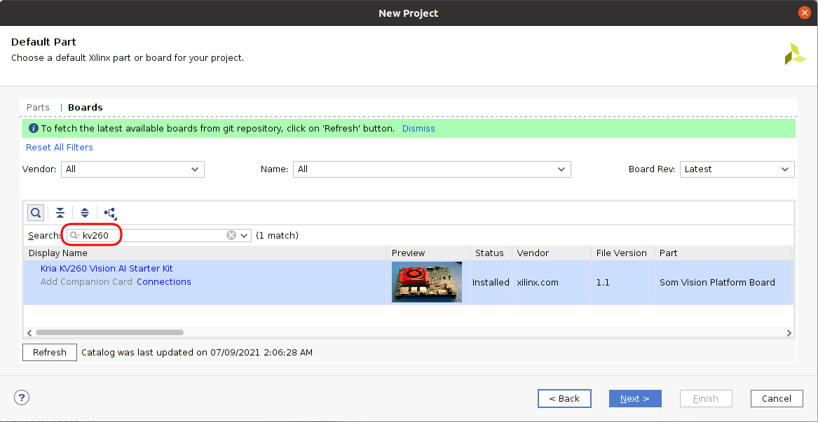
-
New Project Summary -> Finish
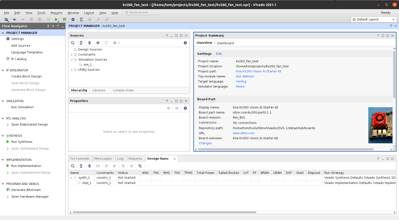
-
Default Project Manager View
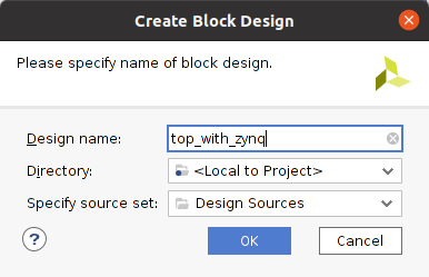
-
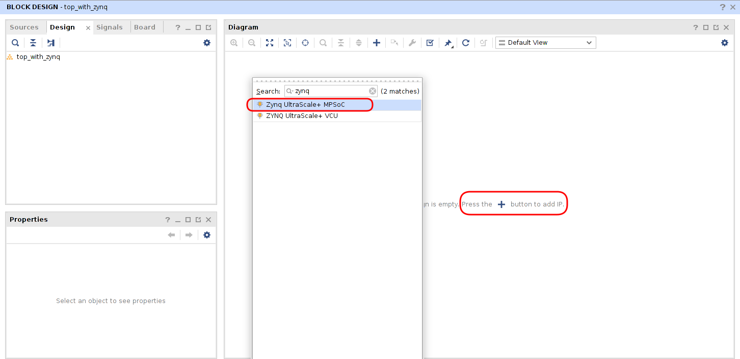
Create Block Design
-
Add Zynq MPSoC IP
-
Unchanged Zynq MPSoC Block
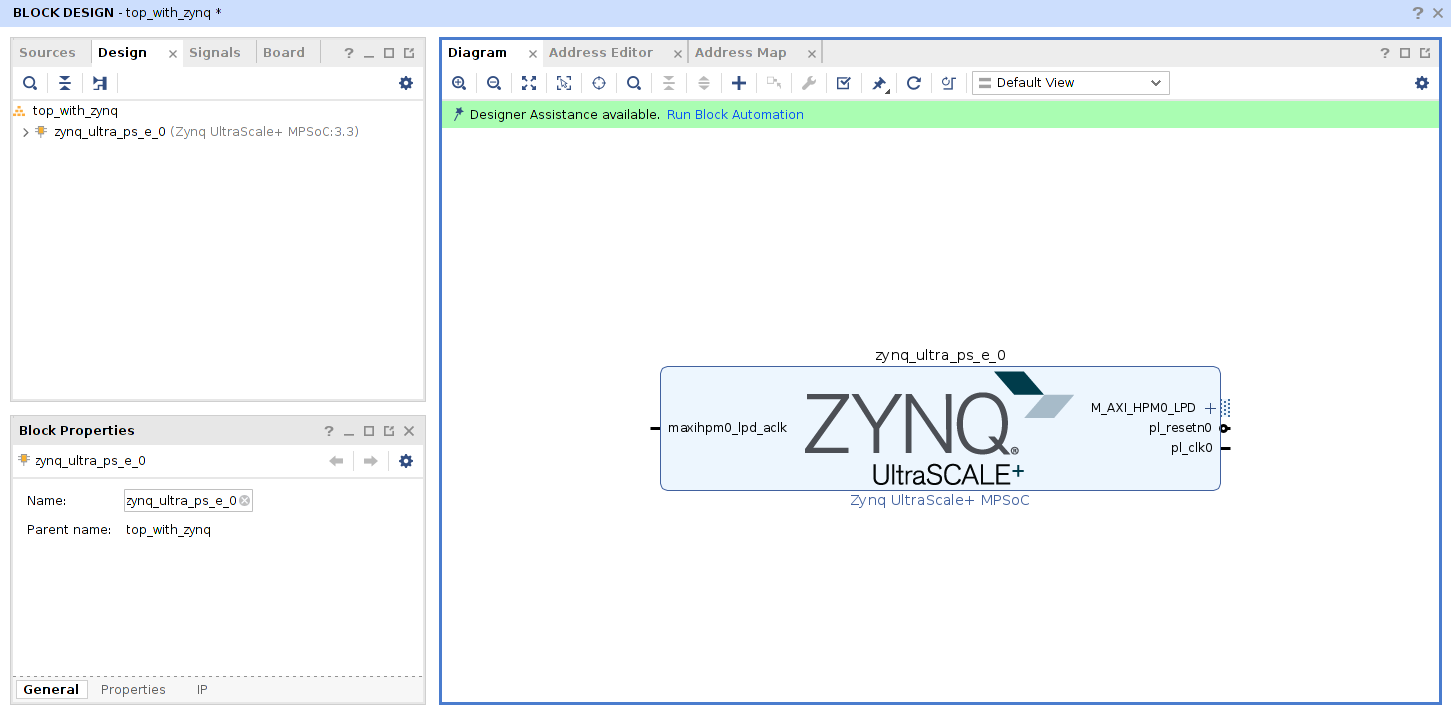
Double click on the MPSoC Block.
-
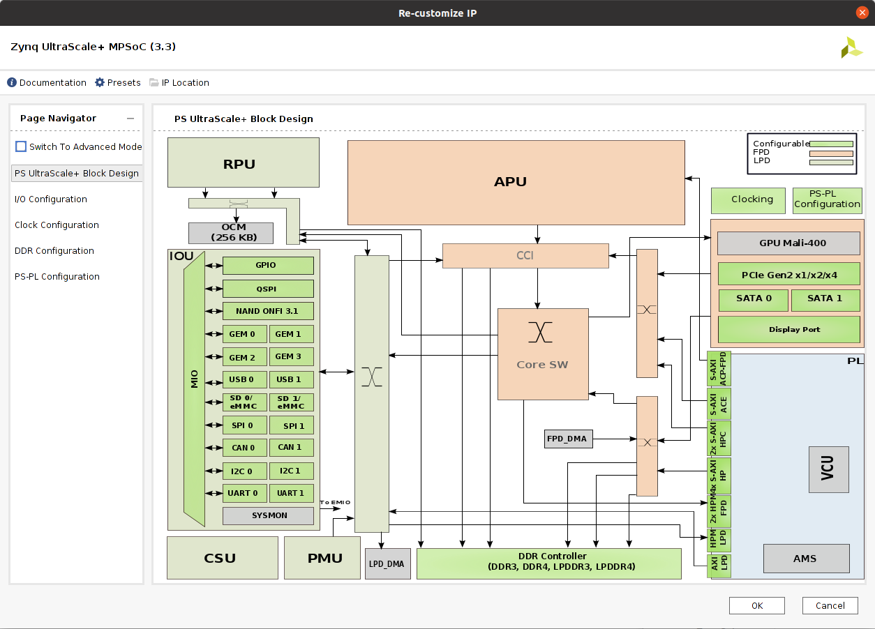
MPSoC Configuration Screen
-
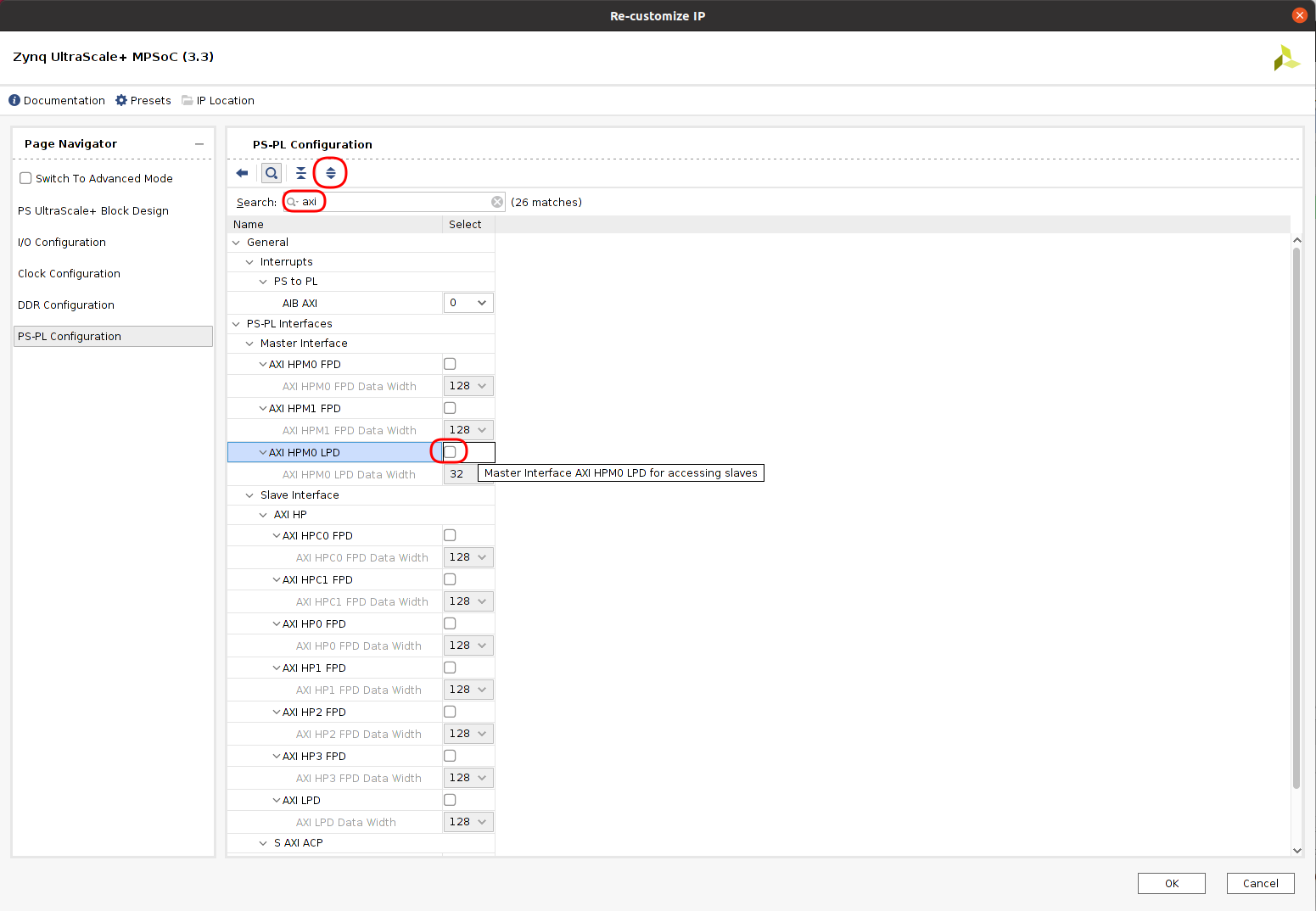
Disable AXI Interface on MPSoC
-
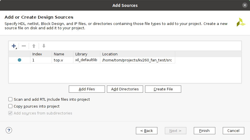
Add Sources
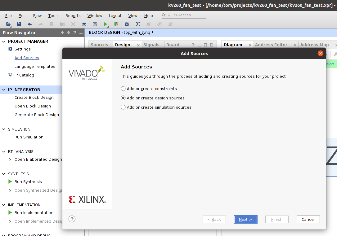
-
Add top.v File
-
Add top.v as module to Block Design
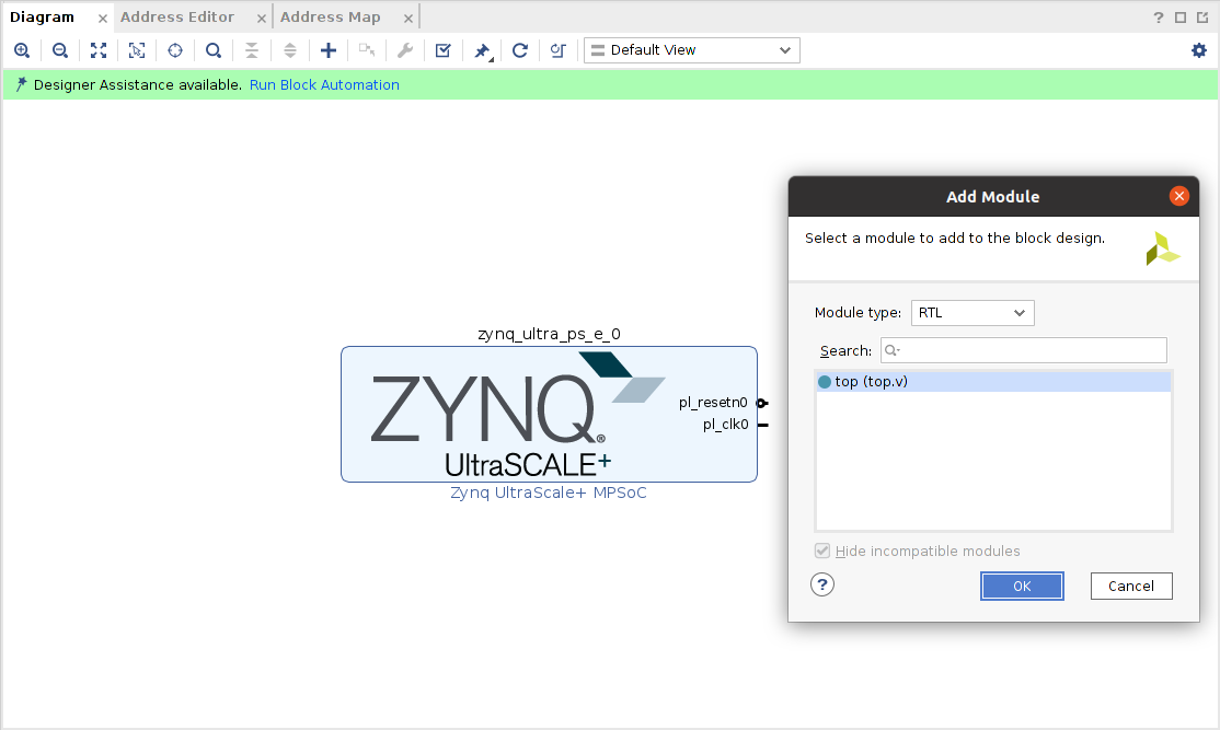
-
Create
fanport
-
Create HDL Wrapper

-
Top is now
top_with_zynq_wrapperdesign
You can change design toplevel by right clicking different design source and selecting "Set as Top"
-
Synthesize the design with Flow -> Run Synthesis (or press F11)
This will take quite a while. Vivado will create a bunch of different tasks called "Design Runs" and execute those in parallel if it can.

-
Do "Run Implementation": Flow -> Run Implementation
This merges all the design information into one FPGA design database.

Select "Open Implemented Design"
-
Assign pin location and voltage to
fanportOpen the I/O Ports tab through the top menu bar: Windows -> I/O Ports

Press [Ctrl-S] to save pin constraints.

-
Do
Run Implementationagain.It will rerun a bunch of steps...
Select "Generate Bitstream" when all is done.
-
Open Hardware Manager when Bitstream generation has completed

-
In Hardware Manager: Open Target -> Autoconnect -> Program Device


If you board booted from an SDCard with PetaLinux (and only then!!!), the fan will now spin on for 6 seconds and then switch off for 2 seconds.
SUCCESS!!!
If you booted the board without an SDCard and without loading a barebones FW somehow, then the PL part isn't activated, and you can't run a bitstream on the FPGA.
-
Zynq UltraScale+ Device - Technical Reference Manual
Required reading for better general understanding of how IOs are mapped etc.