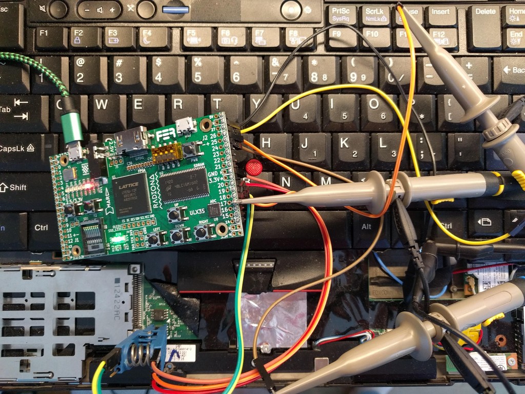
The SPI Spy is an open source (both hardware and software) SPI flash emulation tool. It can store a flash image in the SDRAM connected to the FPGA and serve the image to a host CPU over the SPI bus. This allows you to avoid the lengthy SPI flash erase/write cycles during firmware development as well as to more easily explore early boot time security against TOCTOU attacks.
The design is currently based on the ULX3S which has an Lattice ECP5-12F FPGA and a 16-bit wide 32 MB SDRAM. It might be portable to the TinyFPGA-EX or other open source ECP5 boards, although it uses a custom SDRAM controller to be able to meet the difficult timing requirements of the SPI flash protocol (described below).
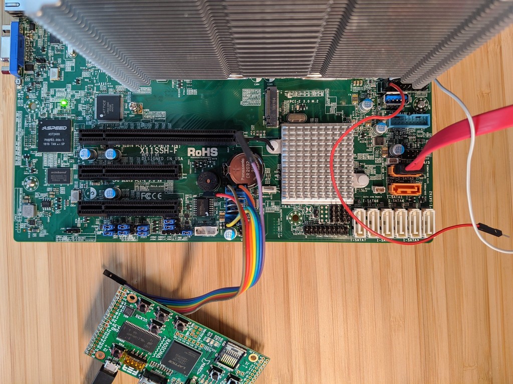
It has been tested on the Thinkpad x230 (no SFDP) and the Supermicro X11SSH-F (with SFDP). Write support is very flaky; the entire state machine needs to be redone (issue #17).
- Single SPI up to 20 MHz clock
- 3-byte addressing (up to 16 MB of flash image)
- High-speed (1 MB/s)
/dev/ttyACM0interface - Serial port updates to the SDRAM (could have a better interface issue #3)
- Logging flash access patterns (could be longer, issue #5)
- SFDP pages (with some caveats)
- TOCTOU changes to the flash image based on read patterns
- Dual- and Quad-SPI (issue #1)
- Multiple
!CSpins (issue #7) - Fast read command (issue #1)
- Erase/Write emulation (issue #12)
- Status registers (partially supported, could be better)
- Block protection bits (maybe worth it, probably not)
- Linux RISC-V core in the FPGA
- Ethernet over USB-CDC-EEM (maybe working on the ulx3s?)
- Default flash image on SD card
- A decent API for TOCTOU exploration
Typical 8-SOIC and 8-DIP flash chips (!RST and Vcc are optional):
                    +------+
   J1 7     !CS 1---| o    |---8  Vcc   J1 + (for low voltage)
   J1 10     SO 2---|      |---7 !RST   J1 11 (optional)
            !WP 3---|      |---6  SCK   J1 8
   J1 GND   GND 4---|      |---5  SI    J1 9
                    +------+
Typical 16-SOIC flash chips (!RST and Vcc are optional):
                   +--------+
           IO3 1---| o      |--16 CLK      J1 8
   J1 +    Vcc 2---|        |--15 SI/IO1   J1 9
   J1 11  !RST 3---|        |--14
               4---|        |--13
               5---|        |--12
               6---|        |--11
   J1 7    !CS 7---|        |--10 GND      J1 GND
   J1 10    SO 8---|        |---9 !WP/IO2
                   +--------+
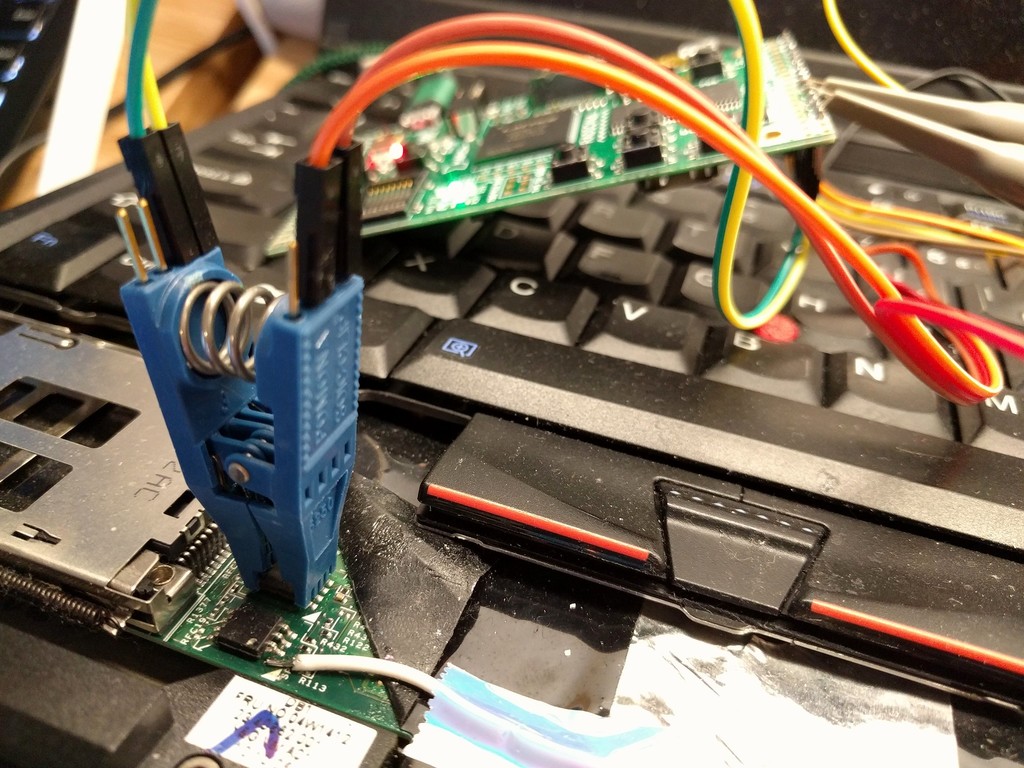
If there is a series resistor on the !CS pin, it might be possible to clip
directly to the chip with a Pomona 8-SOIC "chip clip" and use TOCTOU mode to
override the signal from the PCH. However, this doesn't always work so sometimes
it is necessary to desolder pin 1 from the board, bend the leg upwards and solder
a jumper wire to the pad on the maiboard as shown in the above photo.
If the board has a "Dediprog" or programming header it might be possible to attach directly to the header and also override the chip select pin, although more testing is necessary.
IMPORTANT NOTE the system defaults to using 3.3v signalling for the SPI bus. If you have more modern system, it might use 1.8v and driving it at the higher voltage can cause problems. It is possible to remove the RV3 resistor from the board and provide power to the FPGA GPIO bank through the + pin on the left side connector (J1, pin labeled "2.5/3.3V"); you can connect this pin to the Vcc pin on the SPI flash, which will allow the FPGA to output the same voltage. More details are in issue #10.
If using the spispy with a 3.3V chip and a clip you can leave the Vcc pin
disconnected; otherwise be sure to see the important note above about
hardware changes to support lower voltage flash chips.
Be sure to set the TOCTOU flag in the spispy.v file so that the spispy will
prevent the real flash from responding (or use the #RESET pin; need to
document when this works).
When you plug in the spispy it should show up as a USB-CDC-ACM device with
a device file like /dev/ttyACM0. You might have to start minicom or some
other terminal program to configure the control lines correctly (and to prevent
ModemManager from screwing with it).
Install the sfdp.bin image into the top of DRAM to tell the PCH that the flash
only supports single read commands at the slowest speed:
write-ram 0x1000000 sfdp.bin > /dev/ttyACM0
Install the ROM image into the bottom of DRAM (pv is optional to provide a bargraph
and bandwidth measurement):
write-ram 0x0 coreboot.bin | pv > /dev/ttyACM0
If you want to update part of the ROM image, such as the top 8 MB of the coreboot image,
you can use dd to extract that part:
dd < coreboot.bin bs=1024 skip=8192 | write-ram 0x800000 | pv > /dev/ttyACM0
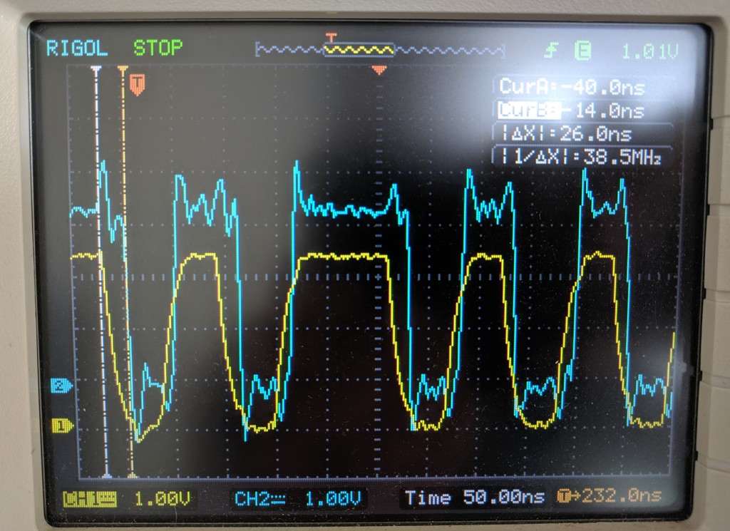
The SPI protocol is difficult to emulate without specialized hardware since it has very demanding timing requirements. The flash device has no control over the clock and must be able to respond to a random read request on the very next clock. At 20 MHz, the slowest SPI bus on some Intel PCH chipsets, this is 50ns from receiving the last bit of the address to having to supply the first bit of the data.
Unfortunately, most microcontroller CPUs aren't able to respond to an incoming SPI byte on the next SPI cycle due to internal muxes and buses, so they aren't able to reply in time. Even if the CPU could do it, most DRAM memory has a 100ns or longer latency for a random read, so it won't be able to answer quickly enough. Additionally, DRAM requires a refresh cycle that takes it offline during the refresh, which adds a random latency.
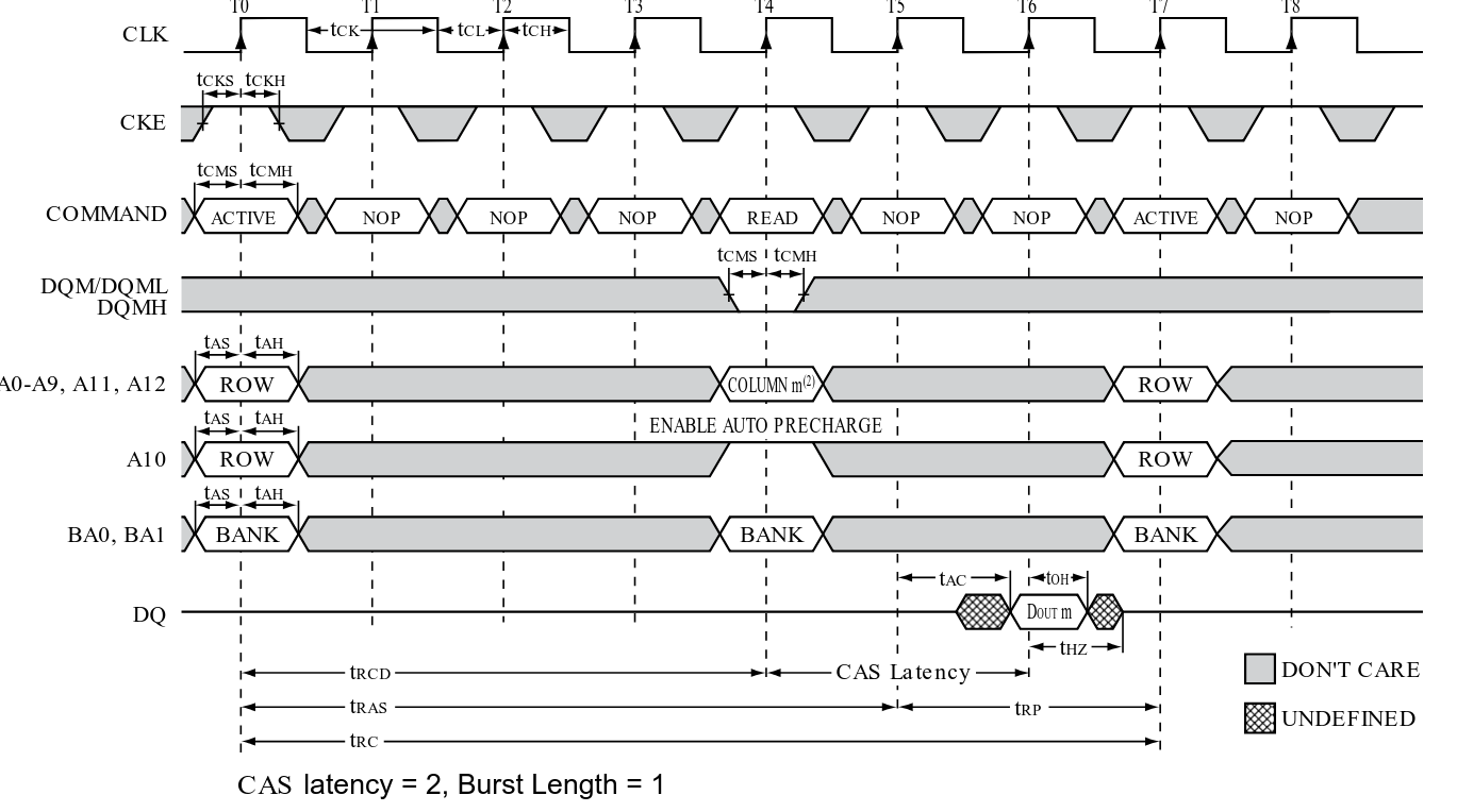
These difficulties can be overcome with an FPGA using a custom DRAM controller. The FPGA is able to inhibit refresh cycles during the SPI critical sections, which reduces the latency jitter, and it can split the DRAM access into two parts: the "row activation" once 16 of the 24 address bits are known, and then a "column read" of two bytes worth of data once 7 of the last 8 bits are known. The correct byte is selected once the last bit of the address has been received.
The row activation command requires at least four DRAM clock cycles, but can be stretched arbitrarily long with a special control signal wired into the FPGA's sdram controller from the SPI bus interface. This allows the FPGA to overlap the activation with the reception of the last bits, and the final column read requires only two clock cycles when the DRAM is configured with a CAS latency of two.
Subsequent bytes are "easy" at 20 MHz for single SPI since the full SDRAM read cycle (7 FPGA clocks) fits into the 8 clocks of the SPI bus (roughly 24 FPGA clocks). For dual or quad-SPI it will be necessary to configure a burst mode on the SDRAM controller or allow new column addresses to be provided dynamically.
