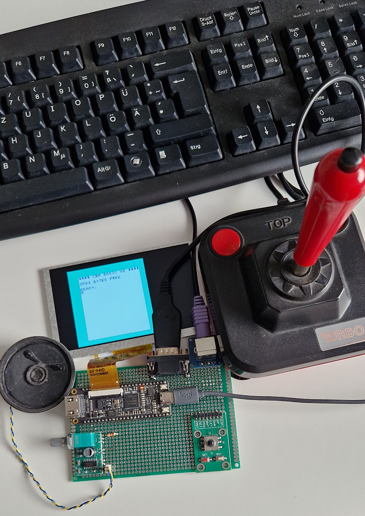
VIC20 living in a Gowin GW1NR-9 FPGA on a Sipeed Tang Nano 9k.
Video output is adapted for a 5" TFT-LCD module 800x480 Type SH500Q01Z (Ilitek ILI6122)
Original VIC-20 core by MikeJ (Mike Johnson) and T65 WoS (Wolfgang Scherr)
Features
- TFT-LCD Video Output
- Speaker Sound
- PS/2 Keyboard
- Joystick
By default cartridge ROM will be booted (see push button how to suppress).
- S1 push button Reset
- S2 Cartridge ROM disable (keep S2 pressed while power-on or excert a S1 push-button Reset, release after)
Prototype circuit with Keyboard and Audio Amp can be powered by Tang USB-C connector from PC or a Power Supply Adapter.
Source code can be synthesized, fitted and programmed with GOWIN IDE Windows or Linux.
Basic testbench as a starting point in the TB folder (vic20_tb.vhd)
Script for compiling the Gowin library, sources and testbench in the simulation folder (sim_vic20.do).
For Simulation run execute_simulation.bat (Windows) or execute_simulation.sh (Linux)
For sake of simplification i use block SRAM resources for all memories (SP, SDP, pROM). In addition rPLL, CLK divdiers and GSR resource.
see pin configuration in .cst configuration file
The bin2mi tool can be used to generate from a 8192 byte Game ROM new pROM VHDL code. For the ROM image i took had to remove the first byte in the generated HEX file indicating the VIC-20 ROM region (0xA0) before providing needed Memory initialization file to the IP Block generator.
- PS/2 keyboard has to be connected to 3.3V tolerant FPGA via level shifter to avoid damage of inputs ! Use e.g. 2 pcs SN74LVC1G17DBVR 5V to 3V3 level shifter. My Keyboard has internal pull-up resistors to 5V for Clock and Data Signals so didn't needed external ones.
- Joystick interface is 3.3V tolerant. Joystick 5V supply pin has to be left floating !
- The FPGA pin delivering SigmaDelta Audio signal to the Amplifier need a low pass filter. 3K3 series Resistor and 4n7 Capacitor to GND.
- Tang Nano 5V output connected to Audio Amplifier and Keyboard supply. Tang 3V3 output to level shifter supply.
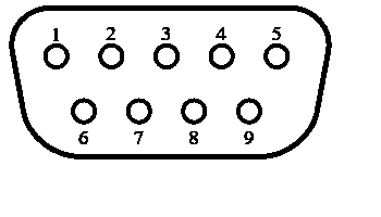
Pinmap D-SUB 9 Joystick Interface

| Joystick pin | Tang Nano pin | FPGA pin | Joystick Function |
|---|---|---|---|
| 1 | J5 8 | 28 | Joy3 RIGHT |
| 2 | J5 7 | 27 | Joy2 LEFT |
| 3 | J5 6 | 26 | Joy1 DOWN |
| 4 | J5 5 | 25 | Joy0 UP |
| 5 | n.c. | n.c. | POT Y |
| 6 | J5 9 | 29 | FIRE B. |
| 7 | n.c. | n.c. | 5V |
| 8 | J6 23 | - | GND |
| 9 | n.c. | n.c. | POT X |
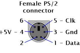
| PS/2 pin | Tang Nano pin | FPGA pin | PS2 Function |
|---|---|---|---|
| 1 | J6 10 | 77 | DATA |
| 2 | n.c. | - | n.c. |
| 3 | J6 23 | - | GND |
| 4 | J6 18 | - | +5V |
| 5 | J6 11 | 76 | CLK |
| 6 | n.c. | - | n.c |
low pass filter for Audio Amplifier input

Sipeed Tang Nano 9k
SH500Q01Z LCD-TFT (Ilitek ILI6122)
D-SUB 9 M connector
Commodore/Atari compatible Joystick
or alternatively 5D Rocker Joystick navigation button module
3K3 Resistor
4n7 Ceramics
Mini PAM8403 Audio Amplifier Module
8R Speaker
PS/2 Keyboard
PS/2 Socket Adapter Module
2 pcs SN74LVC1G17DBVR level shifter
Prototype Board

