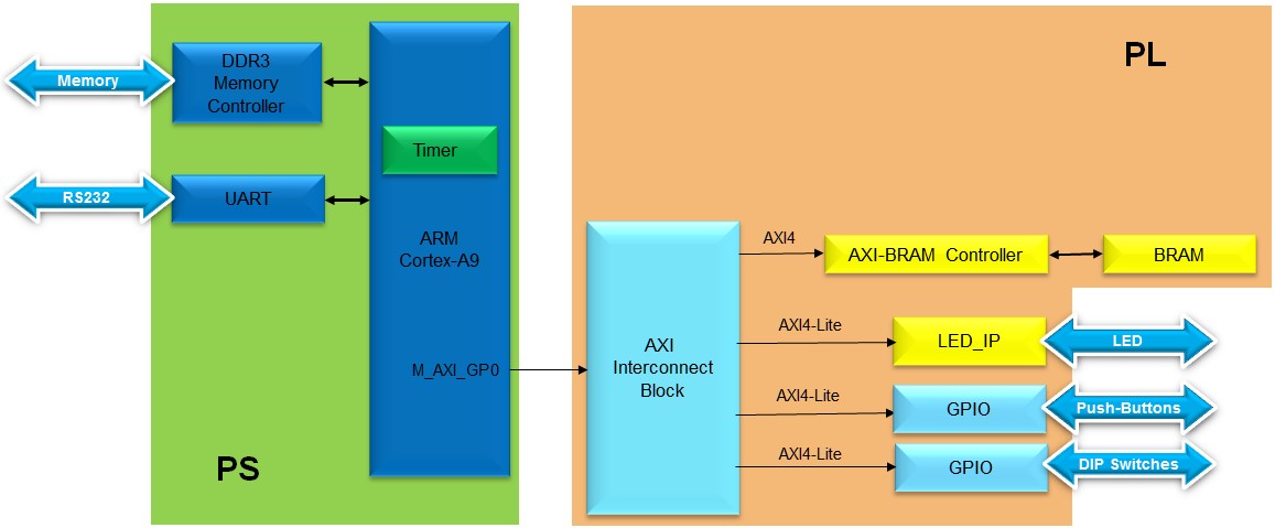
The purpose of the lab exercises of Embedded System Design Flow on Zynq is to walk you through a complete hardware and software processor system design. Each lab will build upon the previous lab. The following diagram represents the completed design of all the labs in this workshop (shown below).
Completed Design
To use the source files for each of the labs in this workshop, you have to download or clone this repository from GitHub.
On the main GitHub webpage for a repository, you can select Clone or download and select Download Zip to download an archive of the repository. You can then extract this to a folder on your local machine.
If you prefer to use git you can clone this repository:
git clone https://github.com/xupgit/Zynq-Design-using-Vivado.git
In the instructions for the labs;
{sources} refers to the ./sources directory in this respoitory once you have copied or cloned it to a local directory.
{labs} refers to the location which you will use as your workspace for the labs in the workshop
NOTE
Board support for the PYNQ-Z1 and PYNQ-Z2 are not included in Vivado by default. The relevant files need to be extracted and saved to:
{Vivado installation}\data\boards\board_files\
These files can be downloaded from
PYNQ-Z1:/board_files.
PYNQ-Z2:/board_files.
PYNQ-Z1/PYNQ-Z2: Connect a micro USB from the board to the PC. Make sure that a jumper is connected to JTAG (between JP1_1 and JP1_2) and another one of them should be connected across the USB pins (between J9_2 and J9_3).
Zybo: Make sure that the JP7 is set to select USB power, and JP5 is set to JTAG. Make sure that a micro-USB cable is connected to the JTAG PROG connector (next to the power supply connector).
ZedBoard: Make sure that two micro-usb cables are used between the PC and the PROG and the UART connectors of the board and that the board is placed in the JTAG mode (MIO6-MIO2 jumpers are in the Dn position).
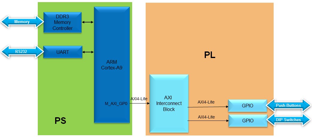
In this lab, you will use IP Integrator to create a processing system based design consisting of the following :
-
ARM Cortex A9 core (PS)
-
UART for serial communication
-
DDR3 controller for external DDR3_SDRAM memory
Processor Design of this Lab
This lab guides you through the process of extending the processing system you created in the previous lab by adding two GPIO (General Purpose Input/Output) IPs.
Extend the System from the Previous Lab
This lab guides you through the process of creating and adding a custom peripheral to a processor system by using the Vivado IP Packager. You will create an AXI4Lite interface peripheral.
You will extend the Lab 2 hardware design by creating and adding an AXI peripheral to the system, and connecting it to the LEDs on the Zynq board you are using. You will use the IP Packager to generate the custom IP. Next, you will connect the peripheral to the system and add pin location constraints to connect the LED display controller peripheral to the on-board LED display. Finally, you will add BRAM Controller and BRAM before generating the bitstream.
Design updated from the previous lab
This lab guides you through the process of writing a basic software application. The software you will develop will write to the LEDs on the Zynq board. An AXI BRAM controller and associated 8KB BRAM were added in the last lab. The application will be run from the BRAM by modifying the linker script for the project to place the text section of the application in the BRAM. You will verify that the design operates as expected, by testing in hardware.
The design was extended at the end of the previous lab to include a memory controller, and the bitstream should now be available. A basic software application will be developed to access the LEDs on the Zynq boards.
This lab guides you through the process of writing a software application that utilizes the private timer of the CPU. You will refer to the timer’s API in the SDK to create and debug the software application. The application you will develop will monitor the dip switch values and increment a count on the LEDs. The application will exit when the center push button is pressed.
You will use the hardware design created in lab 4 to use CPU’s private timer (see Figure). You will develop the code to use it.
Final design


