- Introduction
- Architecture & Organization
- RISC-V CPU
- Versatile Interface Adapter (VIA)
- Direct Memory Access Controller (DMAC)
- uBASIC
- Games
- Memory Map
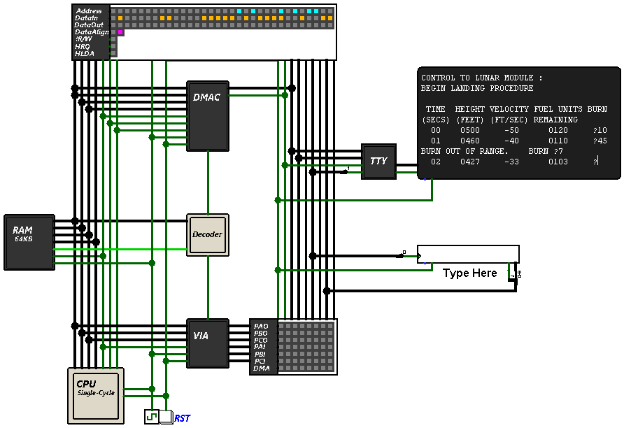
Veecom is a 32-bit computer system that combines the simplicity of 8-bit home computers with modern RISC-V technology, offering users a unique and nostalgic computing experience. It features several notable improvements over the RISC-V Computer 2.0. These include a sleek new design, improved CPU microarchitecture, a new Multi-Cycle CPU version, simplified DMA design, a new replacement for the PIA and a simple BASIC interpreter for an engaging programming experience.
Veecom's design follows a Memory-Mapped approach, utilizing an Address Decoder to access hardware components with a total of 64KB of addressable memory. Notably, Veecom introduces the new Versatile Interface Adapter as a replacement for the Peripheral Interface Adapter (PIA) used in the RISC-V Computer 2.0. It features three 8-bit I/O ports that can be used independently for input or output and a new 8-bit timer with similar functionality to Timer-1 found in the MOS 6522 VIA.
The DMA Controller in Veecom is simpler in design and more compact, supporting up to 64KB of data transfer and addressing capability.
Veecom's CPUs are based on the RV32IM variant of the RISC-V ISA, implementing the 32-bit base integer instruction set alongside the M-extension to support hardware multiplication and division. Additionally Veecom introduces a new Multi-Cycle CPU version, complementing the Single-Cycle and 5-Stage pipeline versions pre-existed in the RISC-V Computer 2.0. The new models feature signficant microarchitectural improvements, bug fixes and an overall cleaner design.
Inspired by the MOS 6522 VIA, Veecom's VIA features several enhancements and improvements over its predecessor, featuring three 8-bit I/O ports Port A, Port B and Port C that can be used for both input and output without the need for data direction register, allowing for more flexible I/O access (Please refer to Memory Map section for supported operations).
Additionally, the VIA features a new 8-bit timer similar to Timer-1 found in the MOS 6522 VIA. it supports multiple operation frequencies (up to f/16, with f/2 set as default) and two operations modes, One-Shot and Free-Run.
The timer consists of an 8-bit latch and an 8-bit counter. The latch is responsible for storing the data that will be loaded into the counter. The Timer Control Register TCR is used to start/stop the timer, configure its operation mode, and set the running clock frequency. Additionally the I/O pin PC7 can be programmed to invert on every time-out.
In One-Shot mode, the content of the latch is loaded into the counter on write, and PC7 is pulled low until the counter reached zero. When the counter reaches zero, the timer expired flag TXP is set and PC7 is pulled back high, the timer counter is not reloaded. However, when the counter value is equal to value stored in the latch, PC7 is pulled low again. If timer output on PC7 is enabled it can be used to generate a programmable pulse width.
In Free-Run mode, the timer expired flag is set and PC7 pin is inverted every time the counter reaches zero, and the content of the latch is loaded into the counter. The timer
continues to decrement from there. If timer output on PC7 is enabled it can be used to generate a square wave.
The Timer Expired Flag (TXP) indicates if a timer overflow has occurred. Once the timer value reaches zero, the TXP flag is asserted and remains asserted unit it is cleared by either reading the flag or writing the Timer Value Register TVR.
This 8-bit register controls the operation of the timer, the following figure lists the functions of the command bits.
The DMA Controller in Veecom is simpler in design and more compact, supporting up to 64KB of data transfer and addressing capability.
The DMA Controller is designed for fast and efficient memory-to-IO data transfer. It features four 8-bit registers: DSL, DSH, DAL and DAH, which control the size and address of the data being transferred (Please refer to Memory Map section for supported operations). The DSL and DSH registers determine the size of the data, allowing for 16-bit transfers. The DAL and DAH registers specify the memory location from which data is fetched. Once the DAH register is written, the DMA Controller asserts the HRQ (Hold Request) pin, signaling the CPU to halt if it's not currently using the system bus. In response, the CPU acknowledges the request by asserting HLDA (Hold Acknowledge) pin. The CPU remains halted until the transfer is completed.
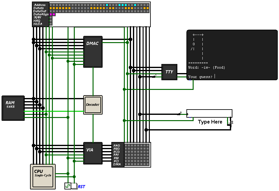
Veecom uBASIC is a derivative of the uBASIC interpreter originally authored by Adam Dunkels. This version of uBASIC has been improved to be made fully interactive, with the incorporation of additional commands and performance optimizations.
Veecom uBASIC supports only the most basic BASIC functionality: IF/THEN, FOR/NEXT, LET, GOTO, GOSUB/RETURN, PRINT, PEEK, POKE and basic mathematical expressions. There is only support for integer variables and the variables can only have single character names. Note that the support for ELSE and CALL statements has been removed.
Veecom uBASIC added support for multiple new commands, these include RUN, LIST, NEW, FRE. making it more interactive and user-friendly.
REM CONFIGURE AND START THE TIMER IN ONE-SHOT MODE
10 LET C = 1
20 POKE 65535, C
30 PEEK 65534, T
40 PRINT T
50 GOTO 30
For more details, please visit Veecom uBASIC repository.
| Address | Symbol | Description | Supported Operations |
|---|---|---|---|
| 0xFFFF | TXP | Timer Expired Flag | Read |
| 0xFFFF | TCR | Timer Control Register | Write |
| 0xFFFE | TVR | Timer Value Register | Read/Write |
| 0xFFFD | PCI | Port C Input | Read |
| 0xFFFC | PCO | Port C Output | Read/write |
| 0xFFFB | PBI | Port B Input | Read |
| 0xFFFA | PBO | Port B Output | Read/write |
| 0xFFF9 | PAI | Port A Input | Read |
| 0xFFF8 | PAO | Port A Output | Read/write |
| 0xFFF7 | DSH | DMA Block Size Hi | Write |
| 0xFFF6 | DSL | DMA Block Size Lo | Write |
| 0xFFF5 | DAH | DMA Block Address Hi | Write |
| 0xFFF4 | DAL | DMA Block Address Lo | Write |
| 0x0000 - 0xFFF3 | RAM | Main Memory | Read/Write |

