This repository contains all the information studied and created during the Advanced Physical Design Using OpenLANE / SKY130 workshop. It is primarily foucused on a complete RTL2GDS flow using the open-soucre flow named OpenLANE. PICORV32A RISC-V core design is used for the purpose.
- Introduction To RTL to GDSII Flow
- About Google SkyWater PDK
- List of All Open-Source Tools Used
- Setting Up Environment
- Day 1 - Inception of open-source EDA, OpenLANE and Sky130 PDK
- Day 2 - Good floorplan vs bad floorplan and introduction to library cells
- Day 3 - Design library cell using Magic Layout and ngspice characterization
- Day 4 - Pre-layout timing analysis and importance of good clock tree
- Day 5 - Final steps for RTL2GDS
- References
- Acknowledgement
RTL to GDSII Flow refers to the all the steps involved in converting a logical Register Transfer Level(RTL) Design to a fabrication ready GDSII format. GDSII is a database file format which is an industry standard for data exchange of IC layout artwork. The RTL to GSDII flow consists of following steps:
- RTL Synthesis
- Static Timing Analysis(STA)
- Design for Testability(DFT)
- Floorplanning
- Placement
- Clock Tree Synthesis(CTS)
- Routing
- GDSII Streaming
All the steps are further discussed in details in the repository.
Google and SkyWater Technology Foundry in collaboration have released a completely open-source Process Design Kit(PDK) in May, 2020. The current release target to a SKY130 (i.e. 130 nm) process node is available as SkyWater Open Source PDK. The PDK provides Physical VLSI Designer with a wide range of flexibility in design choices. All the designs and simulations listed in this repository are carried out using the same SkyWater Open Source PDK.
| Name of Tool | Application / Usage |
|---|---|
| Yosys | Synthesis of RTL Design |
| ABC | Mapping of Netlist |
| OpenSTA | Static Timing Analysis |
| OpenROAD | Floorplanning, Placement, CTS, Optimization, Routing |
| TritonRoute | Detailed Routing |
| Magic VLSI | Layout Tool |
| NGSPICE | SPICE Extraction and Simulation |
| SPEF_EXTRACTOR | Generation of SPEF file from DEF file |
The above list of tools shows that, many different tools are required for various tasks in Physical VLSI Design. Each tool in itself have number of system requirements and require various supporting tools to be installed. Installing each tool one-by-one seems in-efficient. This is made easy by some custom scripts that setup the required tools and environment for them in just a few easy steps. To install all the required tools, one can refer to the below mentioned repositories:
- VSDFlow - Installs Yosys, Magic, OpenTimer, OpenSTA and some other supporting tools
- OpenLANE Build Scripts - Install all required OpenROAD and some supporting tools
During the Physical Designing, one will come across multiple terminologies that are frequently used. Some of them are mentioned below:
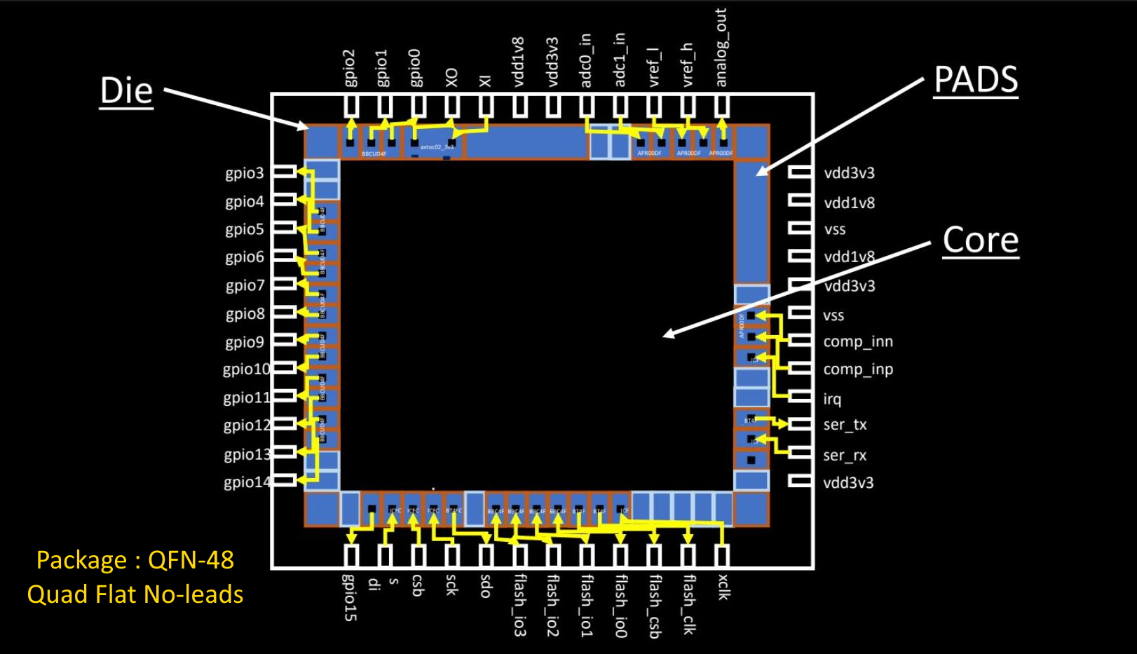
- Package: It is a case that surrounds the circuit material to protect it from physical damage or corrosion and allow mounting of the electrical contacts connecting it to the printed circuit board (PCB). The below snippet shows an IC with 48 pins and Quad Flat No-Leads(QFN) package.
- Die: A die is a small block of semiconducting material on which a given functional circuit is fabricated.
- Core: It is the actual area of the IC where the logic resides.
- Pads: These are the interfaces between the internal signals of a chip and the external pins
RISC-V is a new ISA that's available under open, free and non-restrictive licences. RISC-V ISA delivers a new level of free, extensible software and hardware freedom on architecture.
- It is far simpler and smaller than other commercial ISAs available.
- It avoids micro-architecture or technology dependent features.
- It has small standard base ISA and multiple standard extensions.
- It supports variable-length instruction encoding. A brief design for RISC-V core can be refered here
All the Process Design Kit(PDK) are listed under the pdks/ directory. Along with the Sky130A we are using some other open-source PDKs and other related files are also available in the directory. The location of the PDK directory is given of $PDK_ROOT variable.
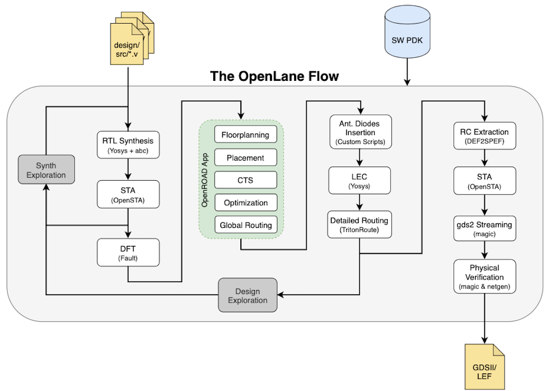
OpenLANE is an automated RTL to GDSII flow which includes various open-source components such as OpenROAD, Yosys, Magic, Fault, Netgen, SPEF-Extractor. It also facilitates to add custom design exploration and optimization scripts. The detailed diagram of the OpenLANE architecture is shown below:
OpenLANE flow consists of several stages. By default all flow steps are run in sequence. Each stage may consist of multiple sub-stages. OpenLANE can also be run interactively as shown here.
- Synthesis
yosys- Performs RTL synthesisabc- Performs technology mappingOpenSTA- Pefroms static timing analysis on the resulting netlist to generate timing reports
- Floorplan and PDN
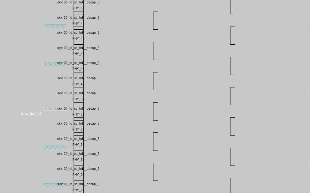
init_fp- Defines the core area for the macro as well as the rows (used for placement) and the tracks (used for routing)ioplacer- Places the macro input and output portspdn- Generates the power distribution networktapcell- Inserts welltap and decap cells in the floorplan
- Placement
RePLace- Performs global placementResizer- Performs optional optimizations on the designOpenPhySyn- Performs timing optimizations on the designOpenDP- Perfroms detailed placement to legalize the globally placed components
- CTS
TritonCTS- Synthesizes the clock distribution network (the clock tree)
- Routing *
FastRoute- Performs global routing to generate a guide file for the detailed routerTritonRoute- Performs detailed routingSPEF-Extractor- Performs SPEF extraction
- GDSII Generation
Magic- Streams out the final GDSII layout file from the routed def
- Checks
Magic- Performs DRC Checks & Antenna ChecksNetgen- Performs LVS Checks
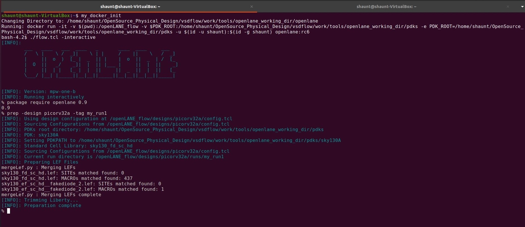
For invoking OpenLANE in Linux Ubuntu, we should first run the docker everytime we use OpenLANE. This is done by using the following script:
docker run -it -v $(pwd):/openLANE_flow -v $PDK_ROOT:$PDK_ROOT -e PDK_ROOT=$PDK_ROOT -u $(id -u $USER):$(id -g $USER) openlane:rc6
A custom shell script or commands can be generated to make the task simpler.
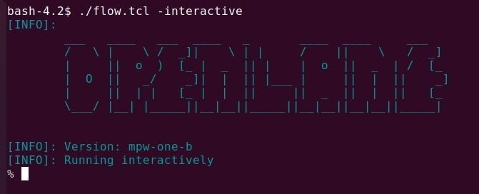
- To invoke OpenLANE run the
./flow.tclscript. - OpenLANE supports two modes of operation: interactive and autonomous.
- To use interactive mode use
-interactiveflag with./flow.tcl
The first step after invoking OpenLANE is to import the openlane package of required version. This is done using following command. Here 0.9 is the required version of OpenLANE.
package require openlane 0.9
The next step is to prepare our design for the OpenLANE flow. This is done using following command:
prep -design <design-name>
Some additional flags that can be used while preparation are:
-tag <name-for-current-run> - All the files generated during the flow will be stored in a directory named <name-for-current-run>
-overwrite - If a directory name mentioned in -tag already exists, it will be overwritten.
During the design preparation the technology LEF and cell LEF files are merged together to obtain a merged.lef file. The LEF file contains information like the layer information, set of design rules, information about each standard cell which is required for place and route.
The first step in OpenLANE flow is RTL Synthesis of the design loaded. This is done using the following command.
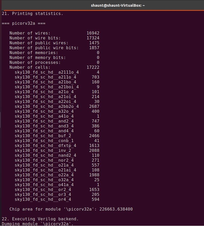
run_synthesis
Chip Floorplanning is the arrangement of logical block, library cells, pins on silicon chip. It makes sure that every module has been assigned an appropriate area and aspect ratio, every pin of the module has connection with other modules or periphery of the chip and modules are arranged in a way such that it consumes lesser area on a chip.
Utilization Factor is ratio of the area of core used by standard cells to the total core area. The utilization factor is generally kept in the range of 0.5-0.7 i.e. 50% - 60%. Maintaining a proper utilization factor facilitates placement and routing optimization.
Power planning is a step in which power grid network is created to distribute power to each part of the design equally. This step deals with the unwanted voltage drop and ground bounce. Steady state IR Drop is caused by the resistance of the metal wires comprising the power distribution network. By reducing the voltage difference between local power and ground, steady-state IR Drop reduces both the speed and noise immunity of the local cells and macros.
Pin placement is a important part of floorplanning as the timing delays and number of buffers required is dependent on the position of the pin. There are multiple pin placement option available such as equidistant placement, high-density placement.
Floorplanning in OpenLANE is done using the following command.
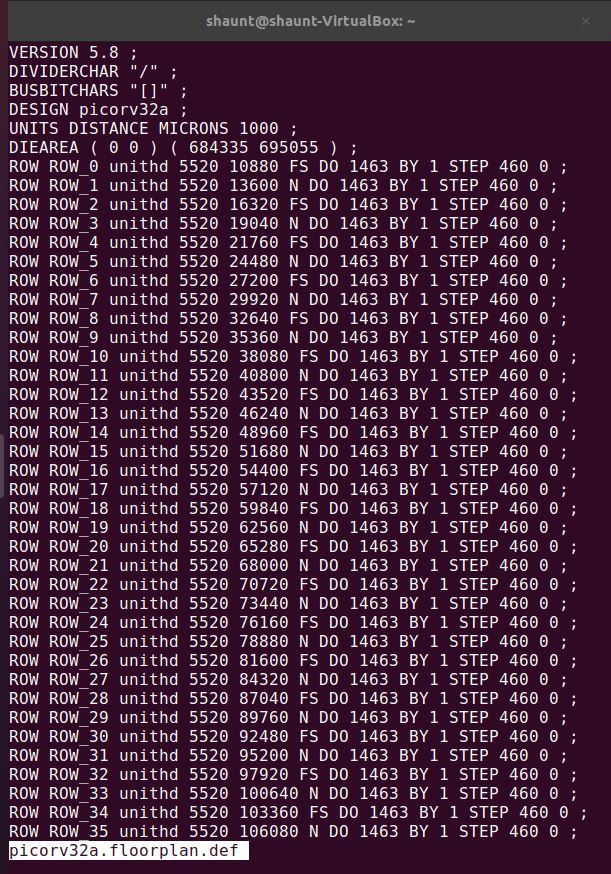
run_floorplan
Successful floorplanning gives a def file as output. This file contains the die area and placement of standard cells.
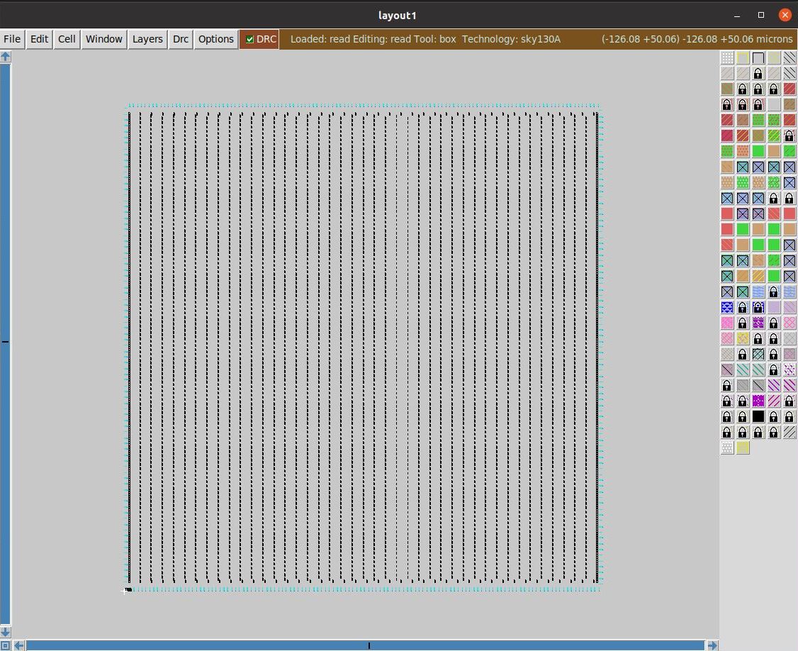
Magic Layout Tool is used for visualizing the layout after floorplan. In order to view floorplan in Magic, following three files are required:
1. Technology File (sky130A.tech)
2. Merged LEF file (merged.lef)
3. DEF File
The next step after floorplanning is placement. Placement determines location of each of the components on the die. Placement does not just place the standard cells available in the synthesized netlist. It also optimizes the design, thereby removing any timing violations created due to the relative placement on die.
Placement in OpenLANE is done using the following command.
run_placement
The DEF file created during floorplan is used as an input to placement. Placement in OpenLANE occurs in two stages:
- Global Placement
- Detailed Placement
Placement is carried out as an iterative process till the value of overflow converges to 0.
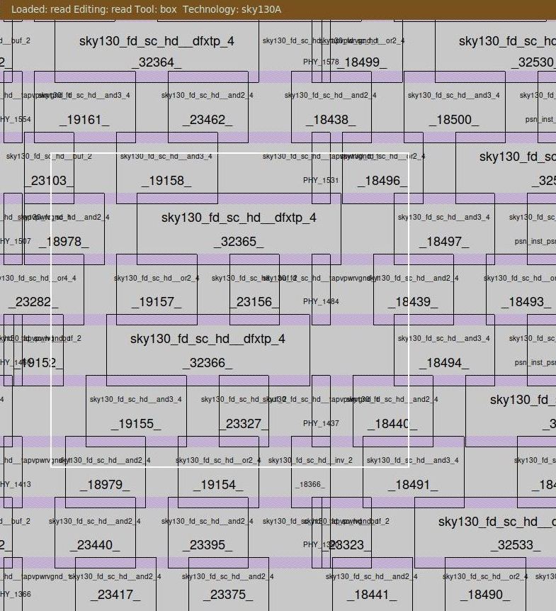 | 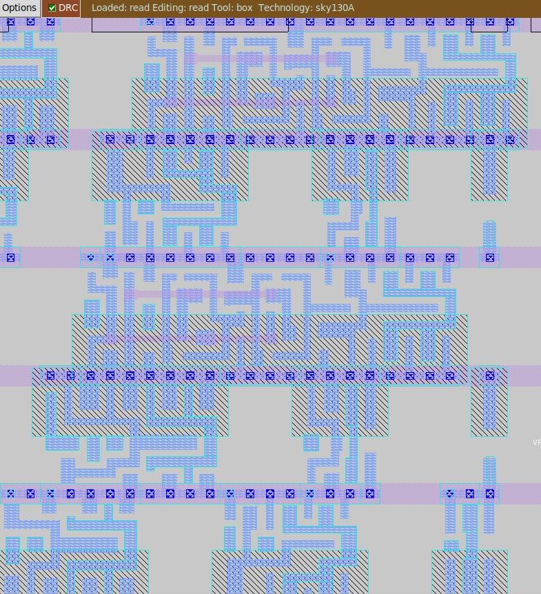 |
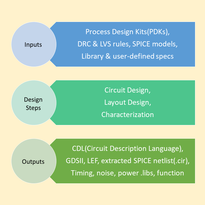
In a border view Cell Design flow is are the stages or steps involved in the entire design of a standard cell. The figure below shows the input, output and design steps involved in cell design
There are few problems of Standard Cells in polygon level format (GDSII). Some of them are:
- Extraction of functionality is complicated and unnecessary as it is known
- Functional/Delay simulation takes way too long
- Power extraction for a whole chip takes too long
- Automatic detection of timing constraints (e.g. Setup time) is difficult
A solution to above problems is Cell Characterization. It is a simple model for delay, function, constraints and power on cell/gate level. The Characterization Flow consists of the following stages:
- Netlist Extraction - Transistors, resistances and capacitances are extracted with special tools and saved as SPICE netlist (or similar)
- Specification of parameters - Library-wide parameters have to be specified: e.g. max Transition time
- Model selection and specification - The used models determine the required data
- Measurement - The cells are simulated with a SPICE-like tool to obtain the required data
- Model Generation - The obtained data is fed into the models
- Verification - Different checks are performed to ensure the correctness of the characterization
Every Design is represented by equivalent cell design. All the standard cell designs are available in the Cell Library. A fully custom cell design that meets all rules can be added to the library. To begin with, a CMOS Inverter is designed in Magic Layout Tool and analysis is carried out using NGSPICE tool.
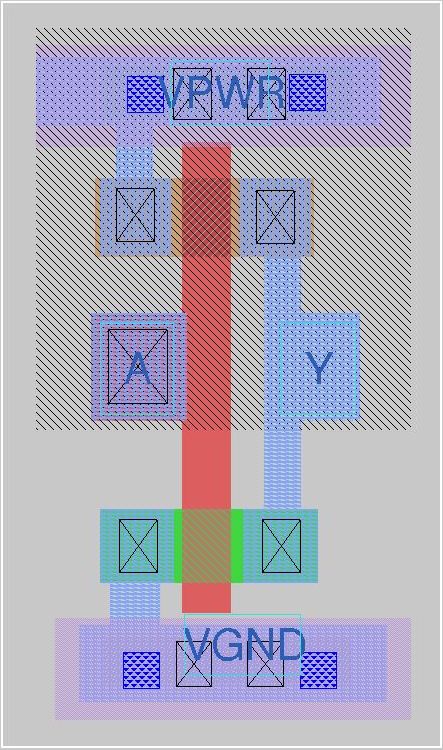
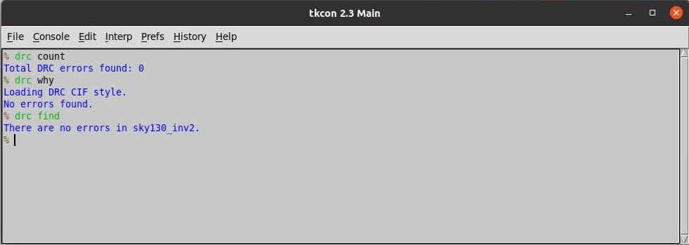
The inverter design is done using Magic Layout Tool. It takes the technology file as an input (sky130A.tech in this case). Magic tool provide a very easy to use interface to design various layers of the layout. It also has an in-built DRC check fetaure.
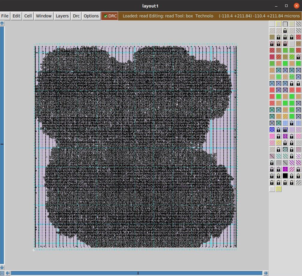
The snippet below shows a layout for CMOS Inverter with and without design rule violations.
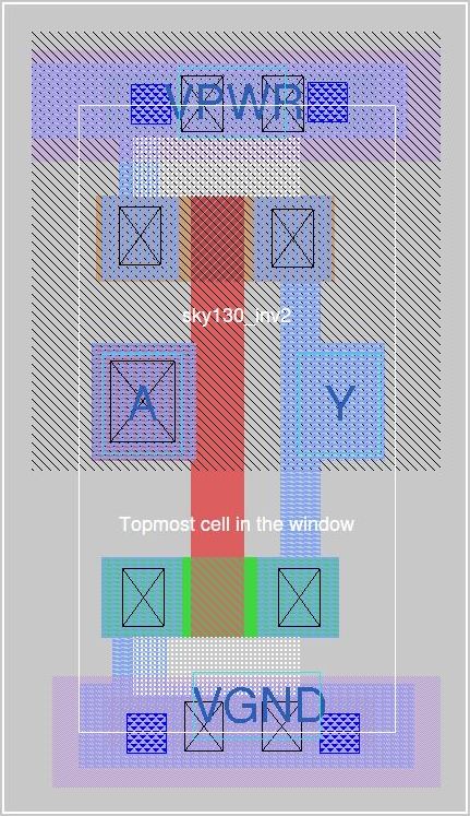 |
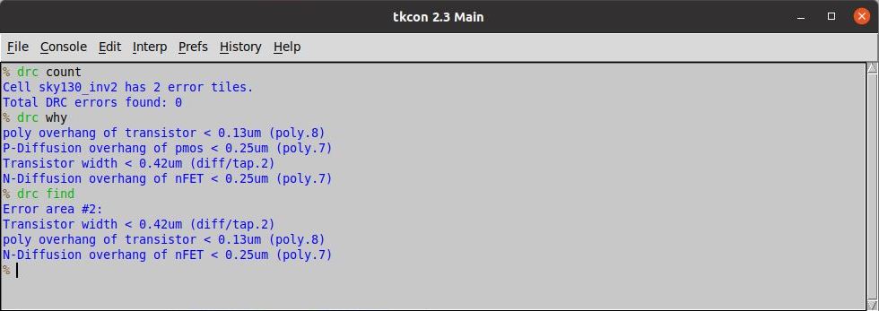 |
 |
 |
To simulate and verify the functionality of the standard cell layout designed, there is a need of SPICE netlist of a given layout. To mention in brief, "Simulation Program with Integrated Circuit Emphasis (SPICE)" is an industry standard design language for electronic circuitry. SPICE model very closely models the actual circuit behavior. Extraction of SPICE model for a given layout is done in two stages.
- Extract the circuit from the layout design.
extract all
- Convert the extracted circuit to SPICE model.
ext2spice cthresh 0 rthresh 0
ext2spice
The extracted SPICE model like the first snippet shown below. Some modification are done to the SPICE netlist for the purpose of simulations, which is shown in the second snippet below.
Commands for Extraction 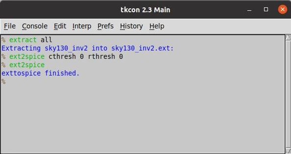 |
.ext file 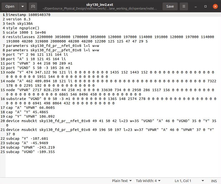 |
Generated SPICE Netlist 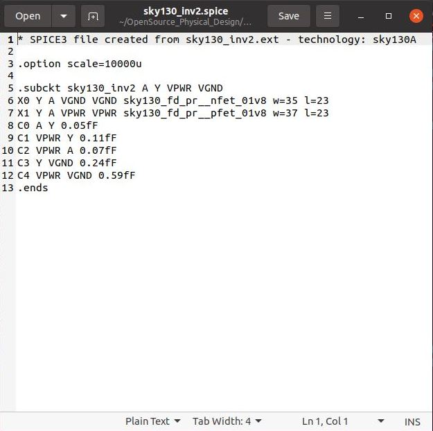 |
Modified SPICE Netlist 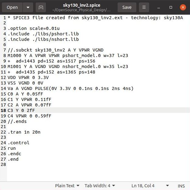 |
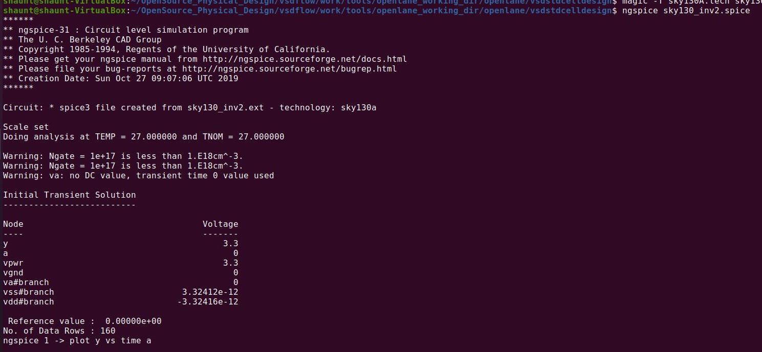
The SPICE netlist generated in previous step is simulated using the NGSPICE tool. NGSPICE is an open-source mixed-level/mixed-signal electronic spice circuit simulator. The command used to invoke NGSPICE is shown below.
ngspice <name-of-SPICE-netlist-file>
Following command is used to plot waveform in ngspice tool.
ngspice 1 -> plot Y vs time A
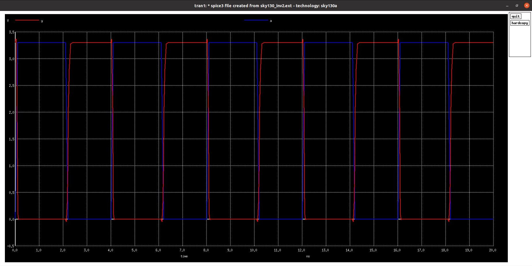
Below figure shows the waveform of Inverter output vs input w.r.t. time. Many timing parameters like rise time delay, fall time delay, propagation delay are calculated using this waveform.
In order to use a design of standard cell layout in OpenLANE RTL2GDS flow, it is converted to a standard cell LEF. LEF stands for Library Exchange Format. The entire design has to be analyzed for any timing violations after addition or change in the design.
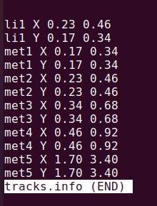
Before creating the LEF file we require some details about the layers in the designs. This details are available in a tracks.info as shown below. It gives information about the offset and pitch of a track in a given layer both in horizontal and vertical direction. The track information is given in below mentioned format.
<layer-name> <X-or-Y> <track-offset> <track-pitch>
To create a standard cell LEF from an existing layout, some important aspects need to be taken into consideration.
- The height of cell be appropriate, so that the
VPWRandVGNDproperly fall on the power distribution network. - The width of cell should be an odd multiple of the minimum permissible grid size.
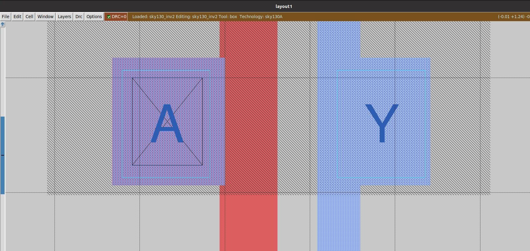
- The input and ouptut of the cell fall on intersection of the vertical and horizontal grid line.
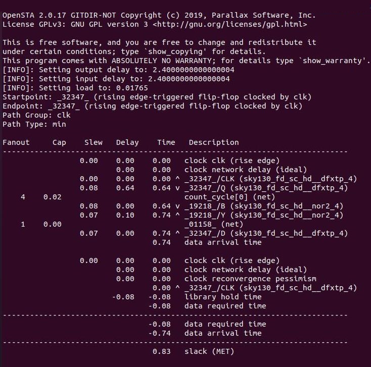
The Static Timing Analysis(STA) of the design is carried out using the OpenSTA tool. The analysis can be done in to different ways.
- Inside OpenLANE flow: This is by invoking
openroadcommand inside the OpenLANE flow. In the openroad OpenSTA is invoked. - Outside OpenLANE flow: This is done by directly invoking OpenSTA in the command line. This requires extra configuration to be done to specific the verilog file, constraints, clcok period and other required parameters.
OpenSTA is invoked using the below mentioned command.
sta <conf-file-if-required>
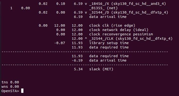
The above command gives an Timing Analysis Report which contains:
- Hold Time Slack
- Setup Time Slack
- Total Negative Slack (= 0.00, if no negative slack)
- Worst Negative Slack (= 0.00, if no negative slack)
 |
 |
If the design produces any setup timing violaions in the analysis, it can be eliminated or reduced using techniques as follows:
- Increase the clock period (Not always possible as generally operating frequency is freezed in the specifications)
- Scaling the buffers (Causes increase in design area)
- Restricting the maximum fan-out of an element.
Clock Tree Synthesis(CTS) is a process which makes sure that the clock gets distributed evenly to all sequential elements in a design. The goal of CTS is to minimize the clock latency and skew. There are several CTS techniques like:
- H - Tree
- X - Tree
- Fish bone
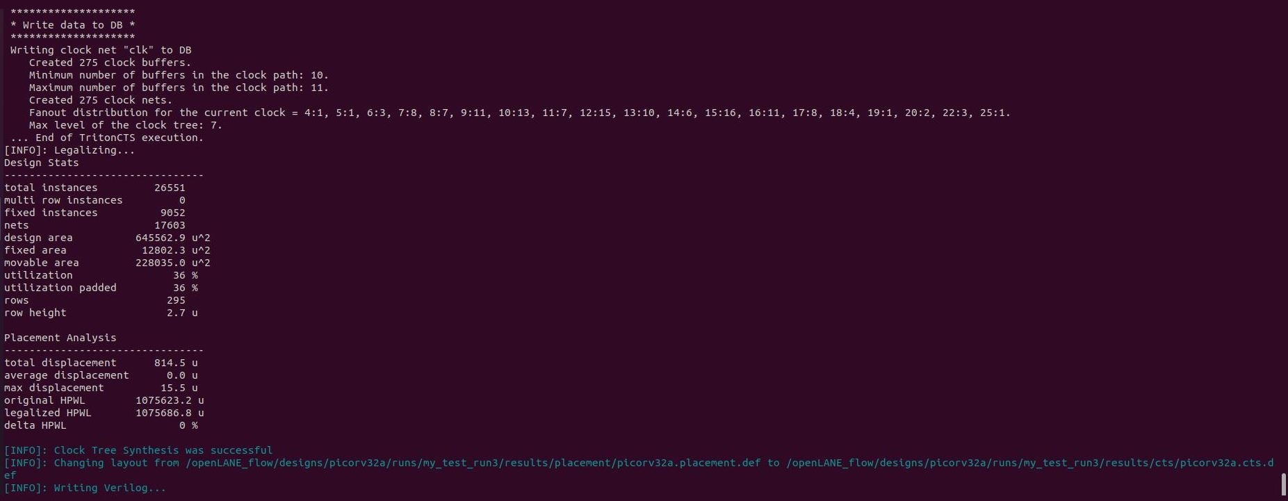
In OpenLANE, clock tree synthesis is carried out using TritonCTS tool. CTS should always be done after the floorplanning and placement as the CTS is carried out on a placement.def file that is created during placement stage.
The command used for running CTS in OpenLANE is given below.
run_cts
In a normal RTL to GDSII flow the generation of power distribution network is done before the placement step, but in the OpenLANE flow generation of PDN is carried out after the Clock Tree Synthesis(CTS). This step generates all the tracks, rails required for routing power to entire chip. Generation of power distribution network is done using following command.
gen_pdn
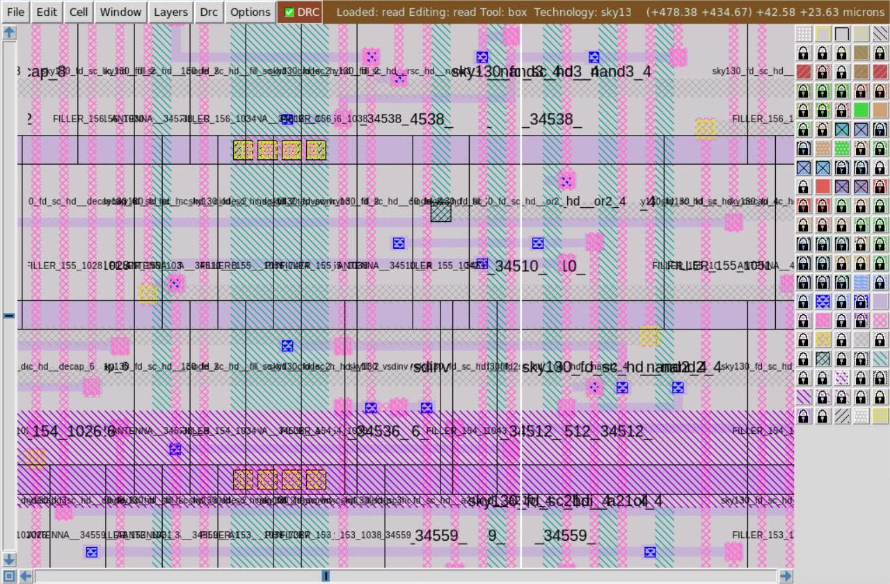
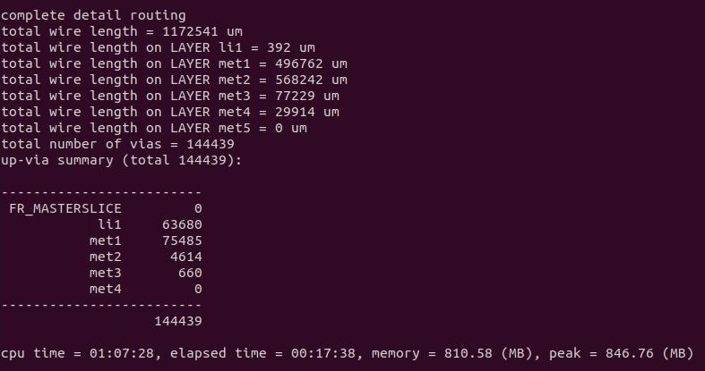
OpenLANE uses TritonRoute, an open source router for modern industrial designs. The router consists of several main building blocks, including pin access analysis, track assignment, initial detailed routing, search and repair, and a DRC engine. The routing process is implemented in two stages:
- Global Routing - Routing guides are generated for interconnects
- Detailed Routing - Tracks are generated interatively. TritonRoute 14 ensures there are no DRC violations after routing.
The following command is used for routing.
run_routing
 |
 |
Standard Parasitic Exchange Format (SPEF) is an IEEE standard for representing parasitic data of wires in a chip in ASCII format. Non-ideal wires have parasitic resistance and capacitance that are captured by SPEF.
OpenLANE consists of a tool named, SPEF_EXTRACTOR for generation of SPEF file. It is a python based parser which takes the LEF and DEF files as input arguments and generates the SPEF file. The following command is used for invoking the SPEC_EXTRACTOR.
cd <path-to-SPEF_EXTRACTOR-tool-directory>
python3 main.py <path-to-LEF-file> <path-to-DEF-file-created-after-routing>
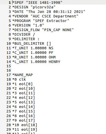
The below snippet shows a small part of the .spef file.
- RISC-V: https://riscv.org/
- VLSI System Design: https://www.vlsisystemdesign.com/
- OpenLANE: https://github.com/The-OpenROAD-Project/OpenLane
- Kunal Ghosh, Co-founder, VSD Corp. Pvt. Ltd.
- Nickson Jose
- Praharsha Mahurkar
- Akurathi Radhika
