Authors:
- Alfredo Paolino
- Vincenzo Petrolo
- Diamante Simone Crescenzo
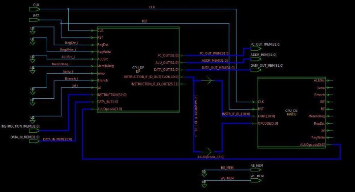
- ALU : It is described, using a mixed behavioral-structural description in order to use the Pentium-4 adder in case of additions or subtractions.
- Register File : It is composed of 32 registers and has 2 read ports and 1 write port.
- Adders : Ripple carry adders used for computing next Program Counter.
- Multiplexers : Are used to choose between input sources in the Register File, Program Counter and ALU.
- Pipeline registers : Are used to store the results from previous stage.
- Size : 2 kB
- Word : 32 bits
- It contains the firmware that is loaded into the microprocessor.
- Asynchronous memory.
- Size : 2 kB
- Word size: 32 bits
- It stores data coming from registers.
- Asynchronous memory.
- LUT size : 62 lines
- Control Word: 9 bits
- Hardwired implementation
- Modular control word generation through std_logic_vector concatenation to improve readability during debugging phase.
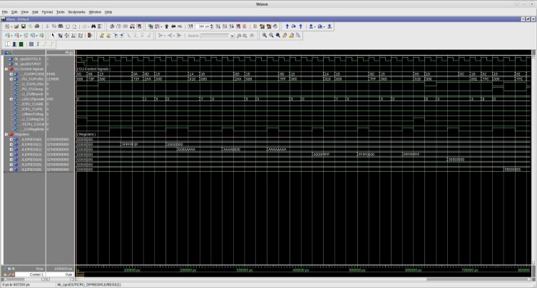
- In order to verify that the instruction set for I- type instructions works, we wrote a simple assembly program that performs:
- Additions;
- Subtractions;
- Mask operations through logical instructions (i.e. AND/OR/XOR etc..).
- Eventually the program halts.
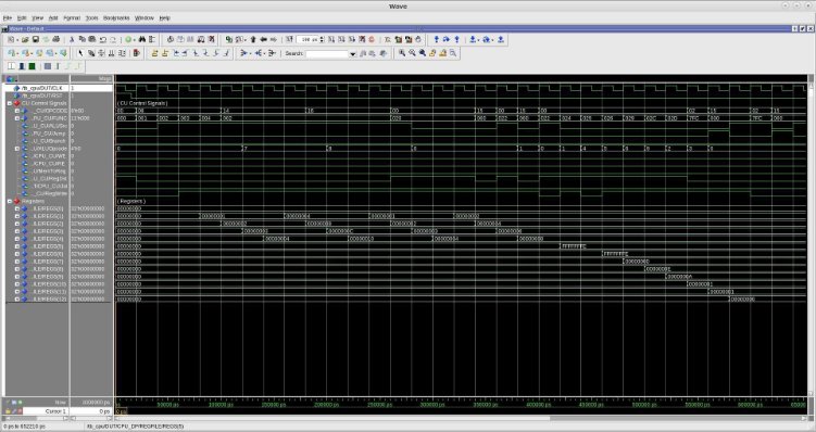
- In order to verify that the instruction set for R- type instructions works, we wrote a simple assembly program that performs:
- Additions;
- Subtractions;
- Shift operations.
- Eventually the program halts.
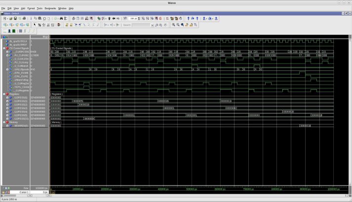
- In conclusion, to create a more complete program we went through the iterative division simulation.
- The algorithm is executed after a call to a procedure (JAL) and performs 81/27.
- When the procedure ends it stores the result into memory and load again into another register. Then it returns to the caller.
- Eventually the program halts.
- Starting from a clock frequency of 50 MHz we reached up to 1 GHz, without major synthesis optimizations.
- Eventually 2 GHz clock frequency goal was achieved using aggressive optimization flow with the usage of compile_ultra, set_dont_touch to avoid removal of skewing registers and set_max_delay to constrain the quasi-critical paths.
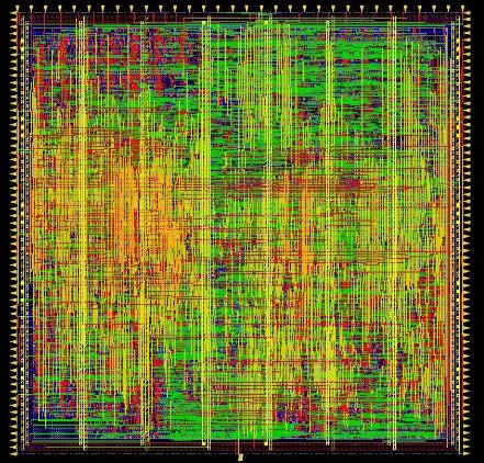
- We followed the flow for the place & route phase.
- After the post-routing optimization phase, we run a static power analysis and got an estimated power of 500 mW running at 1 GHz.
- The total power estimated from PrimeTime (1 GHz) was: 426 mW
- The final step was to produce a report describing more in detail what is shown in this presentation.
For a future version, some of the possible improvements:
- Data Hazard Unit
- Branch Prediction Unit
- Floating Point Unit
- Instruction/Data cache
- Extended Instruction set
- Reducing to 1 the Branch delay slot
- Verification using UVM


