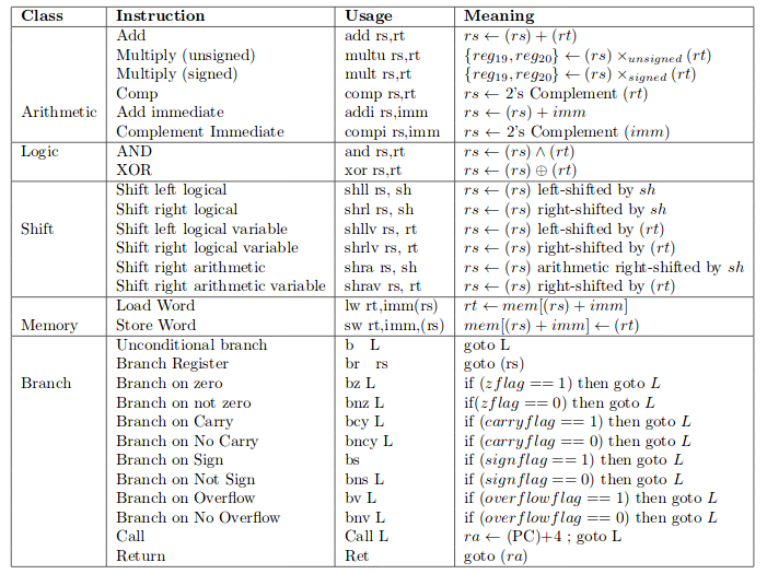
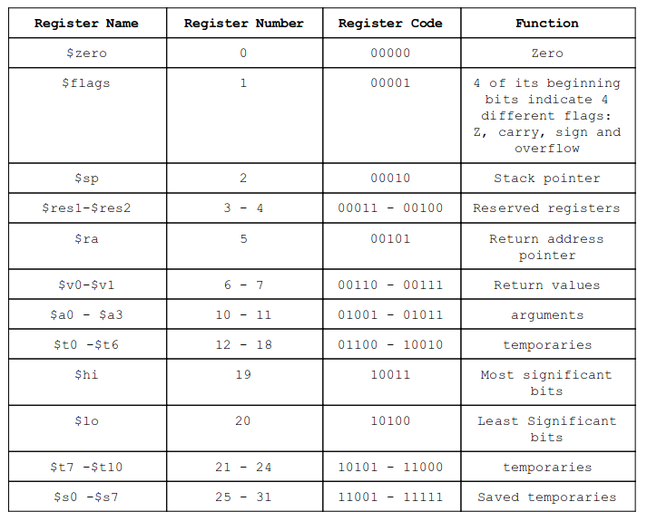
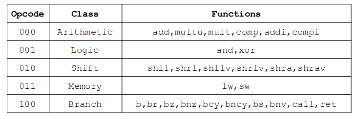
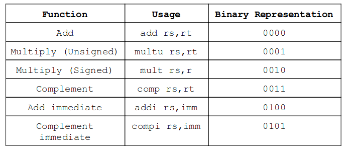
(I made RISC-Fuggit a separate repository to separate the term project from the notes. You can find the notes for MIPS and Verilog in the other repository here)
RISC-Fuggit is the name given to the reduced instruction set computer, designed, implemented and programmed by Nikhil and Amatya. We developed a single cycle instruction execution unit for RISC-Fuggit. The CPU was programmed in verilog with the Xilinx ISE 14.7 and was deployed on the FPGA Spartan 3. Below are the instructions to setup and use this CPU.
-
Xilinx ISE 14.7: ISE Suite 14.7 from Xilinx can be downloaded from their official website. This Video is explains how to download and install ISE 14.7 in Windows 10.
-
FPGA: This is not an essential requirement, you can simulate the CPU using the ISE Suite.
Clone this repository using the following command or download the zip (it's a good habit to star the repo, whenever you fork/clone one!).
git clone https://github.com/itsShnik/COA.git
Move to the directory COA/RISC/RISC_1/ipcore_dir, and click on the file blk_mem_gen_v7_3.xise to open this as a project in Xilinx ISE.
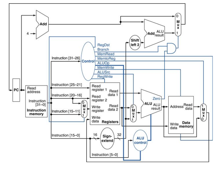
The CPU architechture of RISC-Fuggit is inspired by the image shown below. We have slightly modified this architecture to obtain the required configurations.
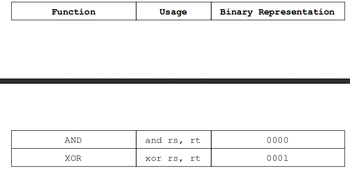
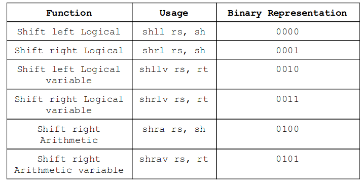
RISC-Fuggit is made of the following components/modules. These modules are instantiated in the main module RISC_main in the following order.
- Instruction Fetch: 1.1. PC Incrementer: Increments the next program counter either by the jump value (L or ra) or one to the current program counter. Works synchronously with the clock. 1.2. Instruction Memory: Loads the instructions atthe current program counter from the BRAM instantiated for instructions only.
- Instruction Decoder: Segments the instruction into interpreteble register addresse, jump values,immediate addresses, operation code and immediatevalues/shift amounts.
- Register Bank: Stores 32 registers each of 32 bits. Writes (on negedge) in values of the input registers on write enable signal. Always outputs values of registers read from instructions.
- Control: Depending on the operation it activates various modules/hardwares with different functionalities (all flags defined later).
- Input Decider: Decides between immediate and register values depending on the instruction type.
- ALU: Main arithmetic and logical unit of the processor, employs hierarchical design incorporating hybrid adders and array multipliers for both signed and unsigned operations.
- Data Memory: Higher level module for BRAM instantiated for data memory.
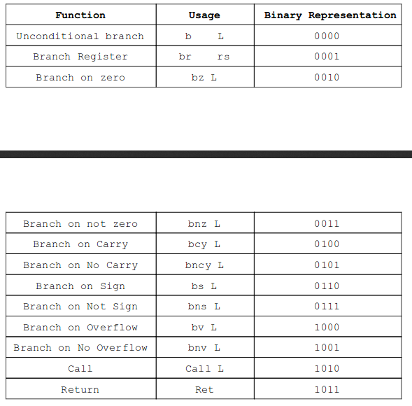
- Branch Logic: Depending on the type of the branch instruction, returns the jump value (relative address of the next instruction).
- Write Back: Chooses between ALU output and memory output to write back to destination register.
- regDst : use when you need three registers to check, which register to write to branch
- memRead: use when data memory is to be read
- memToReg : decide b/w alu ou/p and data memory o/p
- memWrite : select line to data memory
- aluSrc : differentiates between register and constant for ALU
- regWrite : write to reg or not (if write :synchronous)
- regBranch : to decide whether jump to (rs) or L
- raWrite : to decide if it call is used , write back to ra register
- isMult : to write back hi and lo.
- Since it is not mentioned in the assignment the mode of addressing to be used, we have used relative addressing for branch instructions.
- Block RAMs have a peculiar issue that they have significant delay in fetching data (around 0.5 clock cycles) from the RAM. Hence, we have dividedthe input clock into two parts, a slower one and a faster one. The faster one is two times faster and is used to fetch data from Block RAM whereas the slower one is used for other modules.
- Block RAMs have addresses as 0, 1, 2, .... Hence,we have used PC+1 instead of PC+4.
If you are a KGPian, read further. I hope that you are doing well and your semester is going good. If you straighaway want to download this repository and copy, please stop. I am certain that you can do better. A better way to proceed is to use this repository as reference and write the codes yourself. All help that you need is provided in this repository. Just keep in mind the CPU architecture and follow along. If this is the last day of submission and you can't help but copy, go ahead, but don't forget to de-moss. All the best.
