Imitate a read-only SDHCv2 SDcard using FPGAs. It is written according to SDv2.0 specification and has been recognized on SDcard adaptors such as Ugreen, Kawau, SSK, and Realtek PCIe Card Reader.
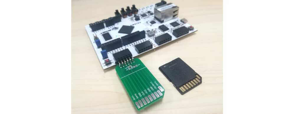 |
|---|
| Figure: FPGA imitated SDcard vs. real SDcard. |
See SDcard.md
Design file sd_fake.v is in RTL directory, which is synthesizable. It allows the FPGA to imitate the behavior of an SDcard, and the SD-host will treat it as a normal read-only SDcard.
 |
|---|
| Figure:sd_fake.v working diagram. |
The figure above is the system diagram when sd_fake is working, the SD-host (blue box) on the left is the SD-host (often an SDcard adaptor or an embedded microprocessor). The SD-host has a SDcard slot and is connected to the SDfake via the 6-wire SD bus.
The SDfake (red box) and the storage (green box) forms a imitated SDcard together. Among them, the storage only provides SDcard's data, the SDfake is to parse and respond the SD bus commands, and when SD-host requests data, the SDfake will read data from the storage and transmit it to the SD-host.
The interface between the SDfake and the storage is a minimalist interface of "given address and get data". Therefore, you can use random access memory to realize the storage, such as on-chip RAM/ROM in FPGA.
The following table describes the module interface of the sdfake.v (omitting some status display signals that are not necessary).
| Type | Name | Direction | Bit Width | Discription |
|---|---|---|---|---|
| reset | rst_async |
input | 1 | Asynchronous reset of the entire SDfake. |
| SD bus | sdclk |
input | 1 | Connect to SD-host. |
| SD bus | sdcmd |
inout | 1 | Connect to SD-host. |
| SD bus | sddat |
output | 4 | Connect to SD-host. |
| Storage interface | rdreq |
output | 1 | Connect to the storage, rdreq=1indicates that the storage needs to be read. |
| Storage interface | rdaddr |
output | 40 | Connect to the storage, give address. |
| Storage interface | rddata |
input | 16 | Connect to the storage, get data. |
| Show status | show_status_bits |
output | 8 | Show SDcard status (unnecessary). |
rst_async is an asynchronous reset signal. When the FPGA starts to work, let rst_async=0 to reset the module, and then let rst_async=1 to release the reset.
SD bus signals include sdclk, sdcmd and sddat, which should be directly led to the FPGA pins and connected to SD-host.
Note: According to the SD protocol, the
sddatsignal is inout, but in sd_fake.v it is output. This is because sd_fake implements an read-only SDcard, which only drivessddatbut never read it.
When SD-host requests data, the sd_fake module fetches data through the storage interface. The wave of storage interaface is shown in the figure below. These signals are synchronized to the clock sdclk. rdreq is the read enable signal. At the rising edge of sdclk, if rdreq has a high-level pulse, the storage data need to be read out to the rddata signal. Then rddata needs to remain unchanged until the next rdreq high pulse.
 |
|---|
| Figure: The storage interface. |
rdaddr signal has an earliness mechanism, that is, the valid address on rdaddr appears several cycles ahead of the rising edge of rdreq, and will remain valid until the falling edge of rdreq. There are two situations:
- When
rdaddrswitches to a new 512B sector,rdaddrwill be valid 8 clock cycles earlier than the rising edge ofrdreq. As shown asaddr0in the figure above. - When the address on
rdaddrbelongs to the same sector as the previous address,rdaddrwill be valid 1 clock cycle earlier than the rising edge ofrdreq. As shown asaddr1,addr2,addr3in the figure above.
The reason why I provide the earliness mechanism of rdaddr is to give enough time to fetch data from the storage, if the storage is a FPGA off-chip storage, such as a NOR-Flash.
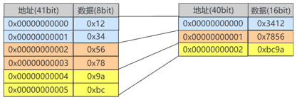
The data signal (rddata) of the storage interface is 16 bits wide, so it is addressed in double-byte. But according to the SDcard specification, the data in the SDcard is addressed in bytes. The conversion method is: a double-byte is divided into two bytes in little-endian, as shown in the figure below.
 |
|---|
| Figure: SDcard addressing vs. the storage interface addressing of sd_fake. |
In double-byte addressing, the address (rdaddr) of the storage interface is 40bit wide, which means that the storage interface has an addressing space of 2*2^40=2TiB, and the address range is 0x0000000000~0xFFFFFFFFFF . However, we obviously won't deploy such a large space (general SDcards are not so large), we need to use the low address of this 2TiB. For example, if only the first 64KiB of the SDcard image is valid (the data bytes after 64KiB may all be 0x00 or 0xFF, which are all invalid or unused space), then we only need to store the data in the FPGA. Deploy a 64KiB ROM (width=2Byte, depth=32768), which takes a address range 0x0000000000~0x0000007FFF.
The signal show_status_bits shows the status of sd_fake, which can be connected to a 8bit LED (not necessary). The following table shows the meaning of each bit.
| Bit位 | 含义 |
|---|---|
| show_status_bits[7] | 0: responsing command 1: idle |
| show_status_bits[6] | 0: sddat in 1-bit mode 1: sddat in 4-bit mode |
| show_status_bits[5] | 0: before soft-reset command 1: after soft-reset command |
| show_status_bits[4] | 0: responsing ACMD 1: not responsing ACMD |
| show_status_bits[3:0] | FSM of sd_fake |
sd_fake can co-simulate with an Verilog SDcard reader. With this simulation, you can see the complete waveform on the SD bus when the SDcard reader reads the SDcard. See anothor project of mine: WangXuan95/FPGA-SDcard-Reader
This repository provides an example project based on Arty development board , which imitate an SDcard with FAT32 file system. When you plug it into the computer through a SDcard adaptor, it can recognize the SDcard and read the file inside.
 |
|---|
| Figure:Windows successfully recognize the FPGA imitated SDcard. |
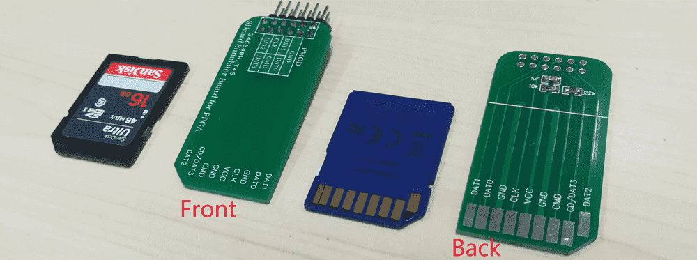
In order to connect the FPGA pins to the SDcard slot, I drew an PCB in SDcard's shape, which has a 2.54mm pin header on the other end. It can be connected to the pin header on the FPGA development board.
 |
|---|
| Figure: SDcard expansion board. |
 |
|---|
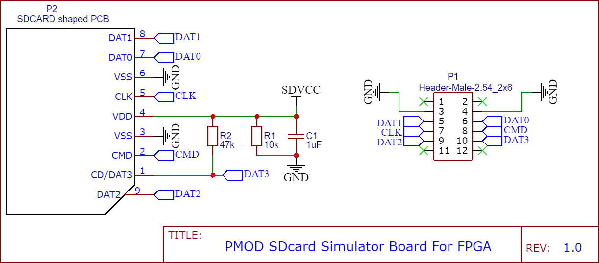
| Figure: Schmatic of SDcard expansion board. |
 |
|---|
| Figure: PCB design of SDcard expansion board. |
Its manufacturing file gerber.zip can be directly provided to PCB manufacturers for proofing. Note that:
- The board thickness must be 1.6mm, which is similar to the thickness of a standard SDcard.
- R1 resistor (10kΩ), C1 capacitor (1uF) are used to generate power supply current. Some SDcard adaptors use power supply current to detect SDcard insertion.
- R2 resistor (47kΩ) is necessary because DAT3 signal also has SD card insertion pull-up detection function.
- SDVCC power supply is provided by the SDcard adaptor, and should not be used to power the FPGA development board. The FPGA should use its own power supply.
- You can use the immersion gold process to make the SDcard's gold fingers more frequently inserted and removed. It is also allowed to not use the immersion gold process, but the plugging life may only be a dozen times.
For Arty development board, when we solder the pin headers, we should use 2x6 double-row bent pins and solder them on the back, as shown below:
 |
|---|
| Figure: Header soldering direction. |
Then plug it into the JD PMOD on Arty board, the direction is shown below:
 |
|---|
| Figure: Connect SDcard expansion board to Arty board. |
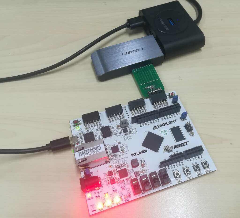
Using Vivado to open the project in the example-vivado directory, compile and program it. Then insert it into an SDcard adaptor. Then the SDcard should be recognized by the computer.
 |
|---|
| Figure: Connect FPGA imitated SDcard to computer through an SDcard adaptor. |
This repository imitates a read-only SDcard, so you cannot modify the files directly in the SDcard recognized by the computer. To modify the files, the only way is to recreate an SDcard image and place it in the ROM described by Verilog code of the FPGA.
Note that in the project's top-level code fpga_example_top.v , besides the sd_fake module, there is a large always block which implements an ROM which stores SDcard data:
always @ (posedge sdclk)
    if(rom_req)
        case(rom_addr)
        40'h00000000df: rom_data <= 16'h8200;
        40'h00000000e0: rom_data <= 16'h0003;
        40'h00000000e1: rom_data <= 16'hd50b;
        40'h00000000e2: rom_data <= 16'hade8;
        // omit 390 lines ... //
        default:        rom_data <= 16'h0000;
        endcase
The data in this ROM comes from a full-disk dump from a real SDcard. For the tutorial, see SDcard.md.
Open the .hex image file that we dumped, you can see the data as shown below. The above ROM code is written according to these data. For example, the address corresponding to 00 82 in the figure below is 0x000001BE . According to the addressing rules of the storage interface, the address in the storage interface is 0x1BE/2 = 0x0DF , so we can get a line of Verilog code: 40'h00000000df: rom_data<=16' h8200; (note that it is 16'h8200 instead of 16'h0082 because of the little endian).
 |
|---|
| Figure: Using Winhex to view the .hex image file that we dumped. |
FPGA 模拟 SDHCv2 版本的只读 SD 卡,依据 SDv2.0 规范编写,已在 绿联 、 川宇 、 飚王 、Realtek PCIe Card Reader 等读卡器上识别。
 |
|---|
| 图:FPGA模拟SD卡 与 真实的SD卡 |
请阅读 SDcard.md
RTL 目录中的 sd_fake.v 就是模拟 SD 卡的设计代码(可综合),它能让 FPGA 模仿 SD 卡的行为,SD-host 会将他视为一张普通的 SD 只读卡。
 |
|---|
| 图:sd_fake.v 工作时的系统框图 |
上图是 sd_fake 工作时的系统框图,左侧 SD-host(蓝色框)是SD卡主机(往往是读卡器、嵌入式微处理器等)。SD-host 具有卡槽,通过SD标准规定的 6 线SD总线与 sd_fake 卡相连。
右侧的 sd_fake(红色框)和存储器(绿色框)共同组成一张模拟 SD 卡。其中,存储器仅仅负责提供数据。sd_fake 负责对SD总线的命令进行解析和响应,并在SD-host 请求数据时,从存储器中读取数据并传给 SD-host。
sd_fake 与存储器之间的接口是一种“给地址即出数据”的极简接口。因此存储器往往选用随机读取存储器,例如FPGA片内RAM/ROM即可。
下表描述了 sd_fake 的模块接口(省略了一部分没必要连接的状态展示信号)。
| 类型 | 信号名称 | 方向 | 位宽 | 描述 |
|---|---|---|---|---|
| 复位信号 | rst_async | input | 1 | 异步复位整个控制器,包括 SD 卡状态 |
| SD总线信号 | sdclk | input | 1 | 连接到 SD-host |
| SD总线信号 | sdcmd | inout | 1 | 连接到 SD-host |
| SD总线信号 | sddat | output | 4 | 连接到 SD-host |
| 存储器接口信号 | rdreq | output | 1 | 连接到存储器,rdreq=1时表明需要读存储器 |
| 存储器接口信号 | rdaddr | output | 40 | 连接到存储器,给出读地址 |
| 存储器接口信号 | rddata | input | 16 | 连接到存储器,读入读数据 |
| 状态展示 | show_status_bits | output | 8 | 展示 SD 卡状态(可以不连接) |
复位信号 rst_async 是异步的,低电平复位的信号。当=0时,SD卡状态全部复位。在 FPGA 开始工作时应该让 rst_async=0 来让 sd_fake 复位一下,之后应该让 rst_async=1 来解除复位。
SD总线信号,包括 sdclk 、 sdcmd 和 sddat,直接引出到FPGA引脚,连接到 SD-host 即可。
注意:按照SD协议,sddat 信号是 inout 的,但 sd_fake 中它是 output,这是因为 sd_fake 实现的是 SD-ROM卡(只读卡),这种卡只会驱动sddat信号,而不会读它。
当 SD-host 请求数据时,sd_fake 模块通过存储器接口取数据。时序如下图,这些信号同步于时钟 sdclk 。rdreq 是读使能信号,在 sdclk 上升沿时,若 rdreq 出现高电平脉冲,则存储器需要将 rdaddr 地址所对应的数据读出到 rddata 信号上。然后 rddata 需要保持不变直到下一个 rdreq 高电平脉冲到来。
 |
|---|
| 图:存储器接口波形图 |
rdaddr 信号具有提前机制,即 rdaddr 出现有效地址比 rdreq 的上升沿提前若干周期,并会保持有效直到 rdreq 下降沿。rdaddr 的提前有以下两种情况:
- 当 rdaddr 切换至某个新的 512B 块(扇区)时,rdaddr 将比 rdreq 的上升沿早至少8个时钟周期有效。如上图中的 addr0
- 当 rdaddr 出现的地址与上一个地址属于同一个扇区时,rdaddr 将比 rdreq 的上升沿早至少1个时钟周期有效。如上图中的addr1、addr2、addr3。
之所以提供 rdaddr 提前机制,是为了给 FPGA 片外存储器(比如NorFlash)足够的时间去取数据。
存储器接口的数据线(rddata)位宽为 16bit,因此以双字节为单位编址。但根据SD卡规范,SD卡中的数据以字节为单位编址。这两者之间的转换方式是:双字节以小端序分割为两个字节,见下图。
 |
|---|
| 图:SD 卡本身的编址规则(左)和存储器接口的编址规则(右)。 |
在双字节编址下,存储器接口的地址 (rdaddr) 位宽为 40bit,这说明存储器接口有 2*2^40=2TiB 的寻址空间,地址范围为 0x0000000000~0xFFFFFFFFFF 。然而我们显然不会部署这么大的空间(一般的SD卡都没这么大),我们需要使用这 2TiB 中的低地址。
比如,如果我们生成的 SD 卡镜像只有前 64KiB 是有有效数据的(64KiB 后面的数据字节可能全都是 0x00 或 0xFF ,都是无效的、未使用的空间),那么我们就只需在 FPGA 里部署 64KiB 的存储器(位宽为 2Byte,深度为 32768),应该占用地址范围 0x0000000000~0x0000007FFF
状态指示信号 show_status_bits 展示 sd_fake 的状态,可以连接到 FPGA 开发板的 8bit LED 灯上,也可以不连。下表展示了每一位的含义。
| Bit位 | 含义 |
|---|---|
| show_status_bits[7] | 低:正在响应命令 高:空闲 |
| show_status_bits[6] | 低:使用1-bit总线 高:使用4-bit宽总线 |
| show_status_bits[5] | 低:未软复位 高:已软复位 |
| show_status_bits[4] | 低:未在进行ACMD 高:正在进行ACMD |
| show_status_bits[3:0] | SD 的初始化状态 |
另外 show_sdcmd_en 、show_sdcmd_cmd 、show_sdcmd_arg 这三个信号用来展示 sdcmd 上的命令字,一般用不到,忽略即可。
sd_fake 可以和一个 SD 卡读卡器的代码进行联合仿真。通过该仿真,你可以看到读卡器读取SD卡时SD总线上的完整波形。仿真工程详见: WangXuan95/FPGA-SDcard-Reader
本库提供了一个基于 Arty 开发板示例工程,模拟一个 FAT32 文件系统的 SD 卡。把它通过读卡器插在电脑上,可以识别出 SD 卡,并读到里面的文件,效果如下图:
 |
|---|
| 图:Windows识别出的 FPGA 模拟的 SD 卡 |
为了能把FPGA的引脚连接到SD读卡器的卡槽上,我画了一个模拟SD卡扩展板,它一端具有SD卡的形状,另一端具有 2.54mm 排针,可以连接到 FPGA 开发板的排母上。
 |
|---|
| 图:模拟SD卡扩展板 |
 |
|---|
| 图:模拟SD卡扩展板原理图 |
 |
|---|
| 图:模拟SD卡扩展板PCB图 |
该板的制造文件 gerber.zip 可以直接提供给 PCB 厂商来打样。制造注意事项:
- 板厚必须是 1.6mm ,这与标准SD卡的厚度相近。
- R1电阻(10kΩ)、C1电容(1uF) 用于产生电源电流,有些读卡器以电源电流为SD卡插入的判据。
- R2电阻(47kΩ) 是必要的,因为 DAT3 信号兼具 SD卡插入上拉检测功能。
- SDVCC电源 由读卡器提供, 不要用来给 FPGA 开发板供电 , FPGA 应该使用开发板自身的电源。
- 可以使用沉金工艺来让 SD 卡的金手指插拔次数更多。也可以不用沉金工艺,但插拔寿命就可能只有十几次,然后就会接触不良,这一点需要注意。
因为我们用的是 Arty开发板 ,在焊接排针时,应使用 2x6双排弯针 ,并且焊接在背面,如下图:
 |
|---|
| 图:排针焊接方向 |
然后把它插在 Arty 开发板的 JD PMOD 上,请注意方向,如下图:
 |
|---|
| 图:Arty开发板与模拟SD卡扩展板的连接 |
用 Vivado 打开 example-vivado 目录里的工程, 编译并烧录。然后把 SD卡转接板插入读卡器,电脑中应该就能识别出 SD 卡。
 |
|---|
| 图:插入读卡器 |
本库模拟的是一张只读的 SD 卡,因此你不能直接在电脑识别出的 SD 卡中修改它。要修改文件内容,只能重新制作 SD 卡镜像,并放在 FPGA 的 Verilog 代码描述的存储器中。
注意到工程的顶层代码 fpga_example_top.v 中除了部署了一个 sd_fake 外,还用一个很大的 always 块实现了一个 ROM (实现了存储SD卡数据的存储器):
always @ (posedge sdclk)
    if(rom_req)
        case(rom_addr)
        40'h00000000df: rom_data <= 16'h8200;
        40'h00000000e0: rom_data <= 16'h0003;
        40'h00000000e1: rom_data <= 16'hd50b;
        40'h00000000e2: rom_data <= 16'hade8;
        // 省略 390 行... //
        default:        rom_data <= 16'h0000;  // .hex 镜像里大多数数据都是 0
        endcase
ROM 中的数据就来自于一张真实的SD卡的全盘导出,导出方法详见 SDcard.md
我导出的 .hex 镜像文件用 Winhex 打开后,可以看到如下图的数据,以上 ROM 代码就是根据这些数据编写的。比如,下图中的 00 82 对应的地址是 0x000001BE ,存储器接口的编址规则,得到存储器接口中的地址是 0x1BE/2 = 0x0DF ,因此得到一行 Verilog 代码: 40'h00000000df: rom_data <= 16'h8200; (注意因为是小端序,所以是 16'h8200 而不是 16'h0082 )
 |
|---|
| 图:用 Winhex 查看 SD卡全盘导出得到的 .hex 镜像文件 |
-9A90FD.svg)


