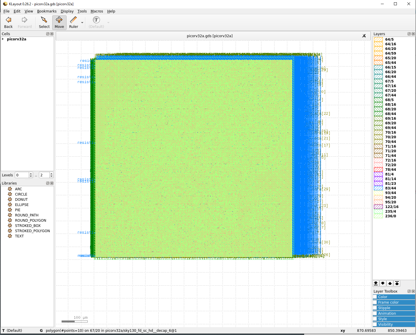
This project is done in the course "Advanced Physical Design using OpenLANE/Sky130" by VLSI System Design Corporation. In this project a complete RTL to GDSII flow for PicoRV32a SoC is executed with Openlane using Skywater130nm PDK. Custom desgined standard cells with Sky130 PDK are also used in the flow. Timing Optimisations are carried out. Slack violations are removed. DRC is verified
- Introduction
- Overall Design Flow
- OpenLane Flow
- OpenLane Installation and Environment Setup
- OpenLane Directory Structure
- Working with OpenLane
- Synthesis
- Floorplanning
- Placement
- Cell Design Flow
- Custom Design of SKY130 Standard cell
- Synthesis, Floorplanning with custom standard cell
- Static Timing Analysis
- Floorplanning and Placement
- CTS
- Pre-CTS Timing Analysis in OpenRoad
- PDN
- Routing
- GDSII
- Acknowledgements
- References
With the advent of open-source technologies for Chip development, there were several RTL designs, EDA Tools which were open-sourced. The missing piece in a complete Open source chip development was filled by the SKY130 PDK from Skywater Technologies and Google. There were several EDA Tools, which played specfic roles in the design cycle. There was not a clean design flow and Skywater pdk was compatible with only the industrty tools. OpenLane addressed these issues in providing a completely automated and clean RTL to GDSII flow. OpenLane is not a tool, but a flow which consists of several EDA tools, automation scripts and Skywater-pdks tuned to work specifically with the open-source EDA tools.
For a design Specification an RTL Design is written in HDLs like Verilog /VHDL or RTL Design is generated using Hardware Construction Languages like Chisel or High Level Synthesis using SystemC, MATLAB HDL Coder, Bluespec etc or a modern abstraction level called TL-Verilog (its not a HDL/HLS) , specified by TL-x.org. After this begins the workflow of taking the RTL Netlist into a fabricated IC, which is called as Physical Design Flow.
Physical Design begins with Floor planning - placing the preplaced cells, power planning etc., secondly Placement of Logical Synthesis. Now we do CTS (Clock Tree Synthesis) such there the skew of the clock is the minimum or within the required threshold. After CTS, Routing is done to route all the components placed. Between each and every step that happens in the physical design flow starting from Logic Synthesis to routing, a procedure called "Static Timing Analysis" is done to analyse the design at every step to ensure the actual correctness of the design. To view every stage, Magic is an open source tool to view the layouts. A small netlist can be extracted and a SPICE Simulation can be performed and compared with the Post Layout Simulation using ngspice.
The RTL Level Design is then synthesized using a Logic Synthesizer. We use Yosys which is an Open Source Logic Synthesizer. The RTL Netlist is then converted into a synthesised netlist where there are details about the standard cells and its implementations. Yosys takes the RTL design and timing .libs and verilog models of standard cells and converts into a RTL Netlist. abc does the tehnology mapping to the required skywater-pdk variants
Different strategies can be used to synthesize for the either the least area or the best timing. To analyse this, synthesis exploration utility generates a report showing the effect on delays/timing/area et.,
This is used to suit the design configuration and generate reports with different metrics to select the best. This is also used for regression testing
This is an optional step carried out by Fault. It is used to test the design
This is done by OpenROAD flow. The macros and IPs are placed in the core before proceding further. This is called as pre-placement. Floor planning is done separately for the macros and it is called macro floor planning. They are placed in such a way that they are closer to the inputs/outputs/other macros where more connections are present. Then to prevent the loading effects de-coupling capacitors are placed so that the logic states are well within the noise margin.
When several blocks tap power from a single source, there is a problem of Voltage Droop at the Vdd and Ground Bounce at the Vss which can again push the logic out of the required noise margin into the undefined state. To mitigate this Vdd and Vss are placed as horizontal and vertical strips in the chip so that the blocks can tap power from the nearest source.
There are two types of placement. The other required logic is placed optimally. Placement is of two steps
- Global Placement- finds the optimal position for each cells. These positions are not necessarly correct, cells may overlap
- Detialed Placement - After Global placement is done minimal alterations are done to correct the issues
To ensure minimum skew the Clock is routed optimally through the circuit using different algorithms. This is done in the OpenROAD flow. This is done by TritonCTS.
Long wires acts as antennas and cause accumulation of charges during the fabrication process damaging the transistor. To avoid this bridging is used to pass the wire through different layers or an antenna diode cell is added to leak away the charges
- OpenLane approach - Insert Fake Diode to every cell input during placement. This matches the footprint of the library of the antenna diode. The Antenna Checker is run to check for violations, if there are violations then the fake diode is swapped with a real one.
- OpenROAD approach - In the global route step, the antenna violation is addressed automatically by inserting an antenan diode OpenLane allows the user to chose either of the above approaches
This step is used to implement the interconnect using the different metal layers specified in the PDK. There are two steps
- Global Routing - This is done inside the OpenROAD flow (FastRoute)
- Detailed Routing - This is performed using TritonRoute outside the OpenROAD flow after the global routing. Before performing this step the Logic Equivalence Check is performed by Yosys, since OpenROAD does some optimisations the circuit.
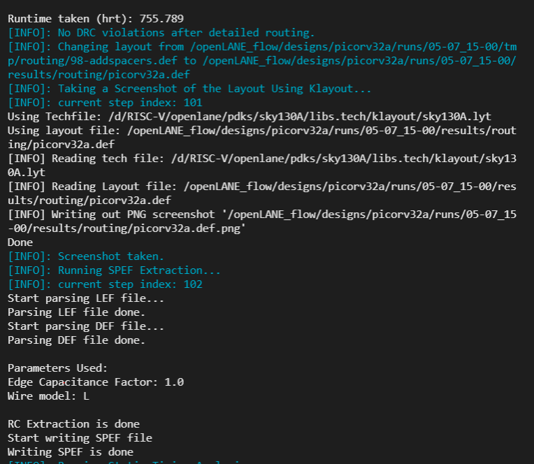
From the .def file, the parasitic extraction is done to generate the .spef file (Standard Prasitic Exchange Format) which produces an accurate analog model of the circuit by including the parasitic effects due to wires, parasitic capacitances, etc.,
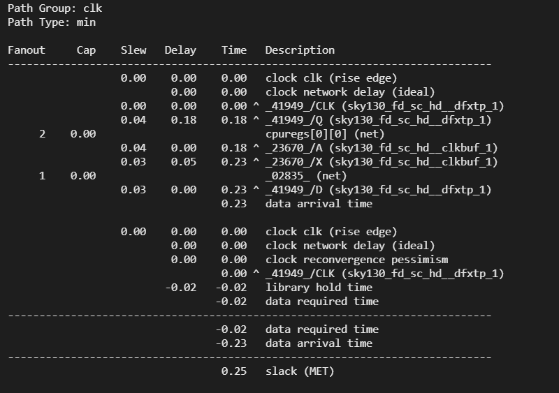
At this stage again OpenSTA is used to perform the Static Timing Analysis.
- Design Rule Check (DRC) is performed by Magic
- Layout Versus Schematic (LVS) is performed by Netgen
The routed .def file is used my Magic to generate the GDSII file
Refer
-
The above repository can be followed if the installation is done on a VirtualMachine/Linux
-
The following steps are required to run OpenLane inWindows Subsystem for Linux (WSL1) before installation of
-
OpenLANE Enable WSL1 -
- Reference
- Install VSCode and RemoteWSL Extension
- Connect to the WSL and open the folder in WSL
- Download and Install VcXserv to run GUI Applications
- Start VcXserv. Check the "Disable access control box"
- Set the Display number as 0 (or anynumber) In WSL terminal use the command
export DISPLAY=:0 - Install Docker Desktop in windows
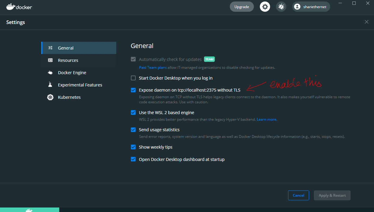
- Enable the below option
- Follow this and install docker dependencies inside WSL
- Every time start docker in WSL to use the docker in windows exposed on the port 2375 using this command
echo "export DOCKER_HOST=tcp://localhost:2375" >> ~/.bashrc && source ~/.bashrcThis must be done everytime before trying to OpenLane Usedocker infoto check the status
This installation can also be done on a remote Linux instance and Putty can be used with X11 fowarding configured to
localhost:0with VcXsrv installed in the host machine with Display number set to 0.
- The
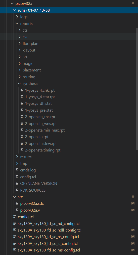
designsfolder contains all the designs provided by Efabless. This is the directory from which OpenLane fetches the design. Consider the picorv32a design. Upon design preparation a runs folder is added. Within the folder containing the date resides the configuration, results, reports and other files that are use in the run.
- The
scriptsfolder contains all the automation scripts used by OpenLane - Open in the
pdkfolder contains three sub folders. skywater-pdkis by defaukt not configured to work with opensource tools. So OpenLane providesopen_pdkandSky130Adirectory which has the configuration files for each of the tools used in the OpenLane flow- The
configurationfolder comtains the .tvl configurations for each tool. However these configurations can be overridden within the design or interactively in the openlane flow - The
pdkdirectory contains
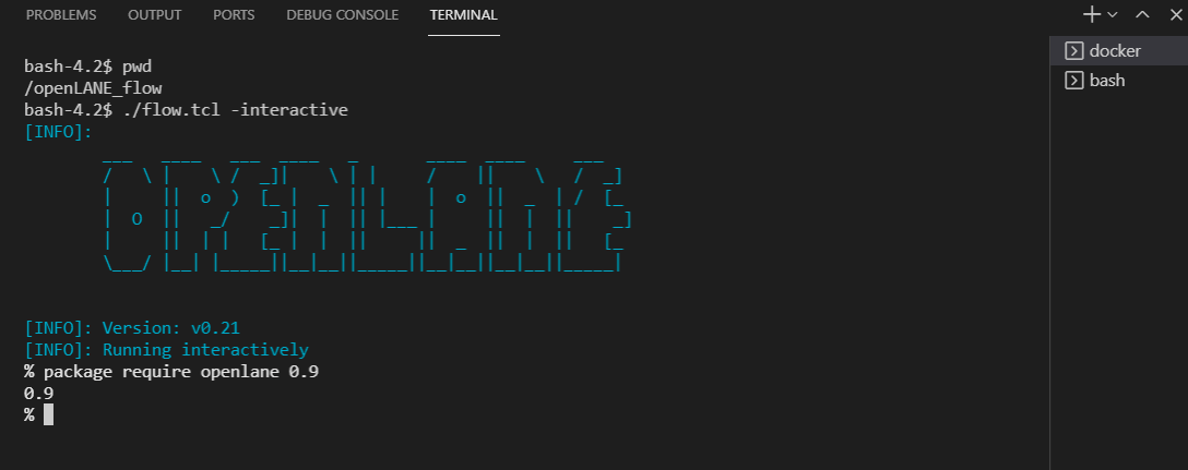
Go the the openlane directory and type docker to start the docker containter.\
The terminal changes into the docker instance.\
Open the OpenLane in interactive mode.\
./flow.tcl -interactive\
Set the package required by OpenLane.\
package require openlane 0.9
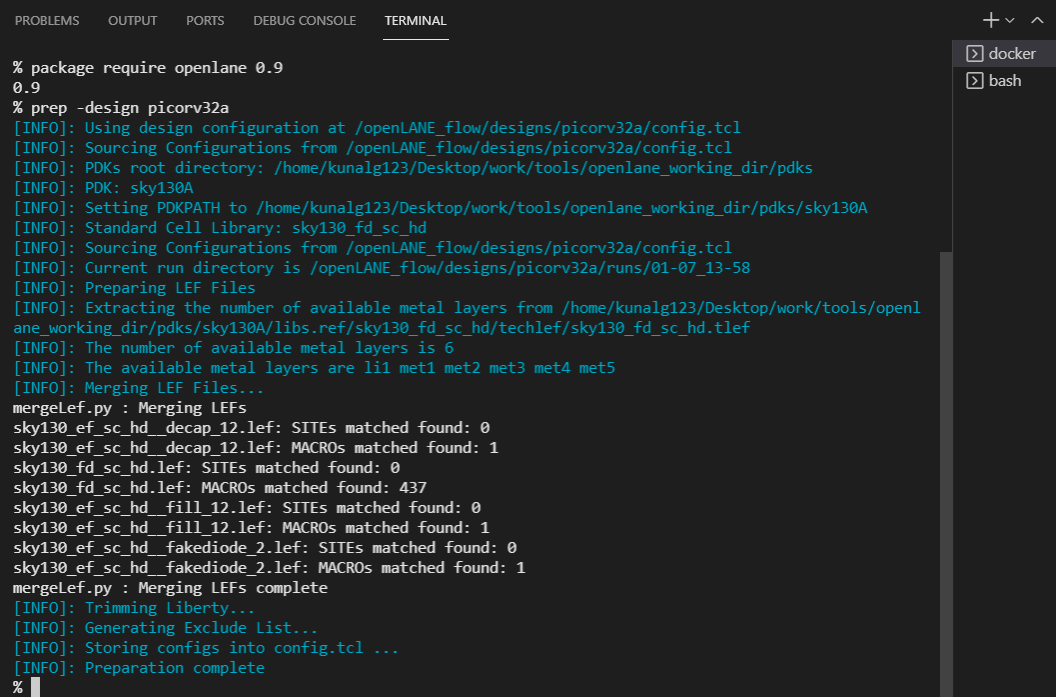
Prepare the design
prep -design picorv32a
- To resume from a previous run use
-tag run_name - To overwrite the previous run use
tag run_name -overwrite - Note: Any configuration done in the
config.tclof the source folder after design preparation will not be refleceted. To run wih a modified configuration, the design configuration can be overriten by passing the configuration to openlane interactively - A runs folder is created as discussed
- On loading a previous run, to know the last run state one has to check the Current def file which is set. This can be done using
echo $::env(CURRENT_DEF)- To set to resume from a stage before the current DEF , one has to set the
CURRENT_DEFenvironment variable to the required path. This can be done using
set ::env(CURRENT_DEF) /path/to/the/required/def/file- The
deffiles of every stage can be found in theruns>results>stage_name>design_stage.defpath. - These
deffiles can be opened withmagicby using thesky130A.techas the technology file and theleffile from thetmpdirectory if required.
Configuration priority (from high to low) is as follows
pdk_specific_config.tcl- Design Folderconfig.tcl- Design Foldertool_specific_config- Configuration Folder in OPENLANE_ROOT
Run the synthesis
run_synthesis
OpenLane invokes the following
Yosys- RTL Synthesis and maps to yosys generic cellsabc- Technology mapping with the Skywater130 PDK. Heresky130_fd_sc_hdSkywater Foundry produced High density standard cells are used.OpenSTA- This does the Static Timing Analysis on the netlist generated after synthesis and generated the timing reports
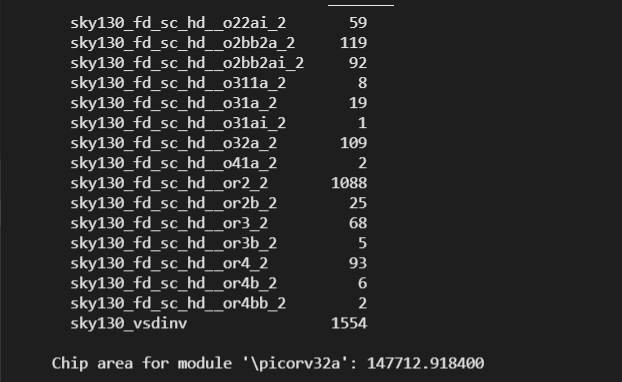
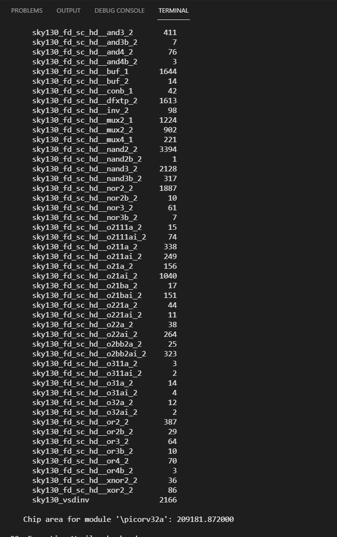
View the synthesis statistics
The STA Reports can be viewed from the Reports folder.
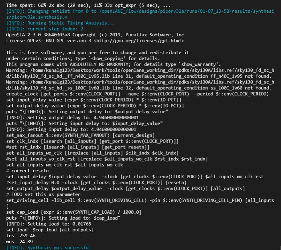
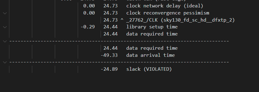
The openSTA tool generated the timing reports. It can be seen from below that
- total negative slack = -759.46
- worst negative slack = -24.89
- The flop ratio is defined as the ratio of the number of flops to the total number of cells
- Here flop ratio is 1613/14876 = 0.1084 (i.e: 10.8%) [From the synthesis statistics]
- The ratio of area occupied by the cells in the netlist to the total area of the core
- Best practice is to set the utilisation factor less than 50% so that there will be space for optimisations, routing, inserting buffers etc.,
- Aspect ratio is the ratio of height to the width of the die.
- Aspect Ratio of 1 indicates that the die is a square die
Floorplanning involves the following stages
-
Whenever there is a complex logic which is repeated multiple times or a design given by a third-party it can be perceived as abstract black box with input and output ports, clocks etc .,
-
These modules can be either macros or IP
- Macro - It is a module such as CPU Core which are developed by the entity fabicating the chip
- IP - It is an "Intellectual Propertly" which the entity fabricating the chip gets as a package from a third party or even packaged Hard IPs developed by the same entity. Common examples of IPs are SRAM, PLL, Protocol Converters etc.,
-
These Macros and IPs are placed in the core at first before placing the standard cells and power planning
-
These are optimally such that the cells which are more connected to each other are placed nearby and oriented for input and ouputs
- The power lines can have some RLC component causing the voltage to drop at the node where it enters the Blocks or the ground of the cell can be at a higher potential than ideally 0V
- When this happens, there is a chance such that the logic transitions are not to the upper or lower noise margins but to the forbidden state causing the circuit to misbehave
- This is prevented by adding a capacitor in parallel with the power and ground node of the block such that the capacitor decouples the block from the power source whenever there is a logic transition
- When there are several cells or blocks drawing power from the same power rail and sinking power to the same ground pin the following effects are observed
- Whenever there is alogic transition from 1 to 0 in a large number of cells then there is a Voltage Droop in the power lines as Voltage Drops from Vdd
- Whener there is a logic transition from 0 to 1 in a large number of cells simultaneously causes the ground potential to raise above 0V calles as Ground Bump
- These effects pose a risk of driving the logic state out of the specified noise margin.
- To avoid this the Vdd and Gnd are placed as a grid of horizontal and vertical tracks and the cell nearer to an intersection can tap power or sink power to the Vdd or Gnd intersection respectively
- The input, output and Clock pins are placed optimally such that there is less complication in routing or optimised delay
- There are different styles of pin placement in openlane like
random pin placement,uniformly spacedetc.,
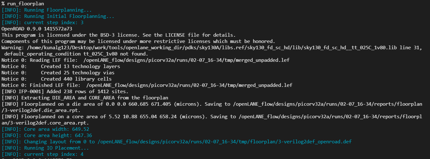
Command: run_floorplan
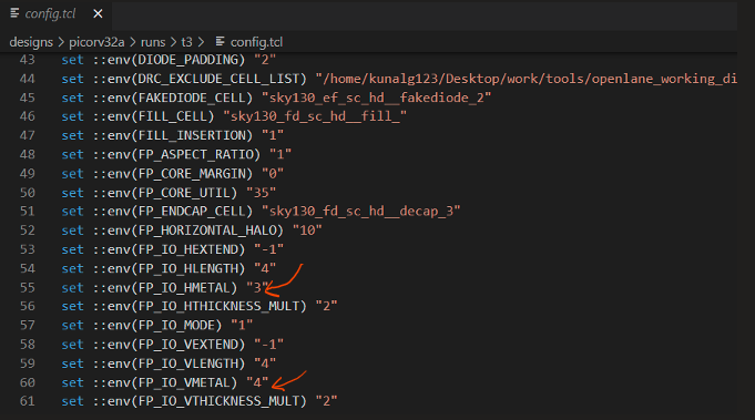
Let us change the VMETAL and HMETAL Layers
Note : In openlane the layer numbers are 1 less than the actual layer
[Right: Modifed Configuration in design, Left: Default Config in openlane]
Run the floorplan
Configuration reflected in the runs folder
This command generated the picorv32a.floorplan.def file in the ./results/floorplan directory
Open the file in magic
magic -T /path tosky130A.tech file in libs.tech magic/
In the tkcon window read the lef and def file as follows. The lef file is present in the tmp directory as merged.lef
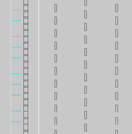
Zoom in view that the pins are equally spaced
- Tap calls are used to avoid Latchup connections
- They connect the nwell to the Vdd and Substrate to Gnd
- In the lower left corner some standard cell buffer are placed even though placement is not done
Floorplan Design Exchange File
- In this steps the standard cells are placed in the floorplanned design
- In palcement buffers are placed whereever the wire delay is large
- Placement in openlane happens in two steps
- Global Placament
- Detailed Placement
- Global placement is not always legalised
- However, Detailed placement is strict and adheres to the Design Rules
Command : run_placement
Output : picorv32a.placement.def file in the results/placement and captures a screenshot and saved the PNG
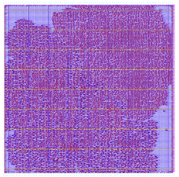
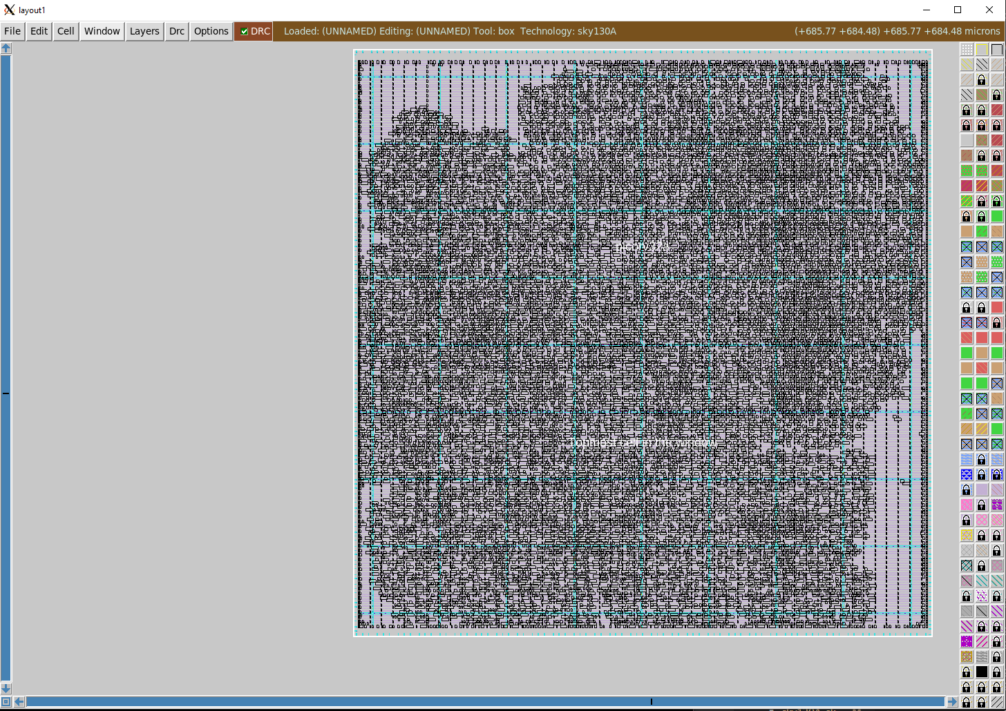
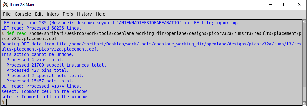
Open the picorv32a.placement.def in magic
- Inputs : PDK, DRC & LVS rules, SPICE models, library & User defined specs
- The introduction of lambda based design rules allowed a design to be loosely tied with the fabrication process
- The layout geometry (DRC) are expressed in terms of multiples of lambda which is half the feature size
- Users define the cell height to be the separation between the power and the ground rail
- Cell width is dependent on the timing information and required drive strength
- Cell Width increases, Area Increases, Timing decreases, Drive Strength increases as the Resistance and Capacitance decreases(RC)
- Supply voltage is also specified by the top level design
- The designed cell must fit in the above specifications
- Output : CDL(Circuit Description Language), GDSII(Graphic Design Standard 2), LEF(Layout Exchange Format), .lib containing Timing, Noise and Power characteristics
- Process
-
Circuit Design
- The function is implemented interms of MOSFETs and a network graph is drawn for PDN and PUN
- The Euler Path is identified for PUN and PDN
- The w/l ratio of the mosfets are decided
- The output we get is interms of a Circuit Description Language
-
Layout Design
- Based on the Euler Path a stick diagram is drawn and the layout is drawn in
magic - DRC is verified in magic
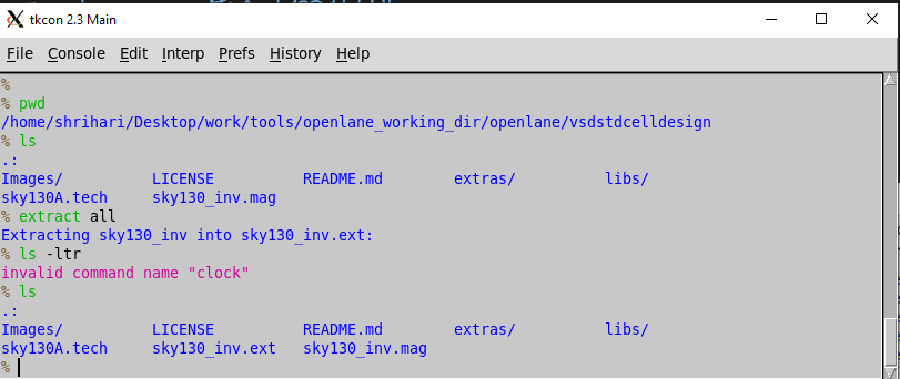
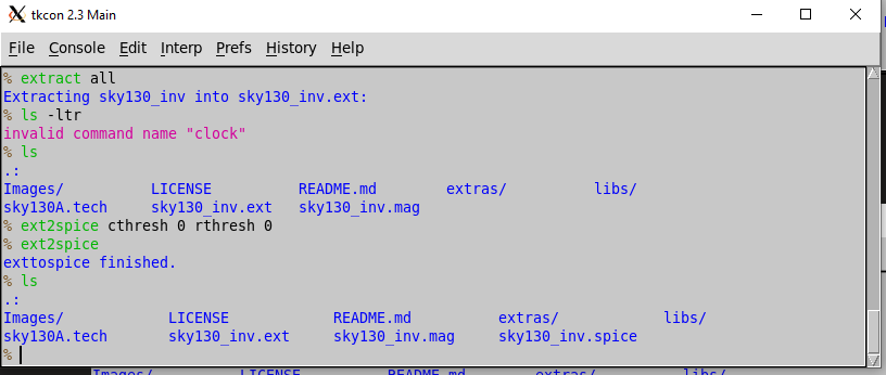
extract allcommand is used to extract the.extfileext2spice cthresh0 rthresh0and RC model spice extraction is done
- Based on the Euler Path a stick diagram is drawn and the layout is drawn in
-
Charactersisation
- Modify the
.spicefile with the necessary power sources - Add the library files and pmos, nmos models
- Add Stimulus commands
- Obtain
- slew_low_rise_thr (20% of max)
- slew_high_rise_thr (80%)
- slew_low_fall_thr (20%)
- slew_high_fall_thr(80%)
- in_rise_thr
- in_fall_thr
- out_fall_thr
- out_rise_thr
- Calculate
- Slew_x = difference between slew_high_x_thr and slew_low_x_thr
- Delay_x = difference between out_x_thr and in_x_thr
- Modify the
-
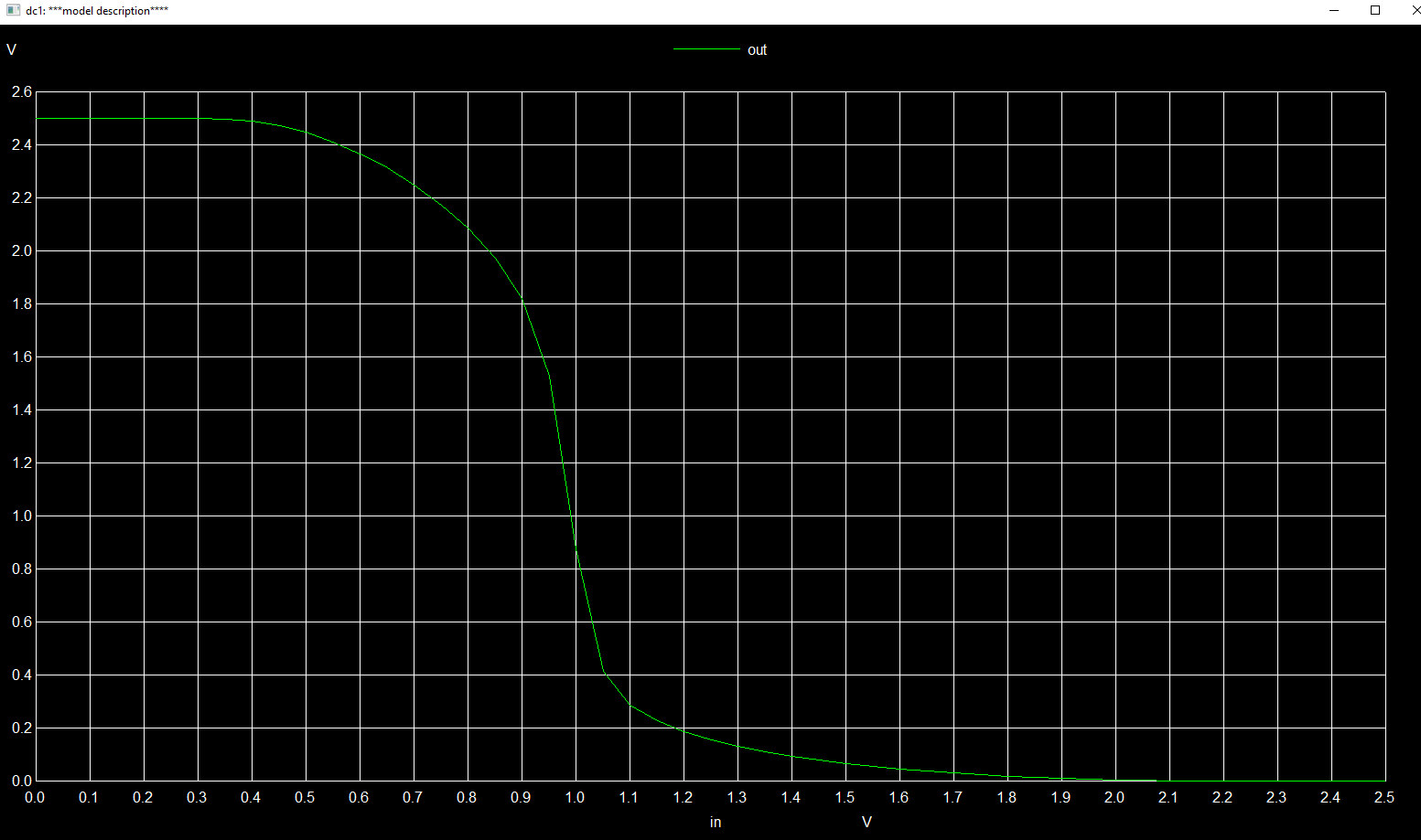
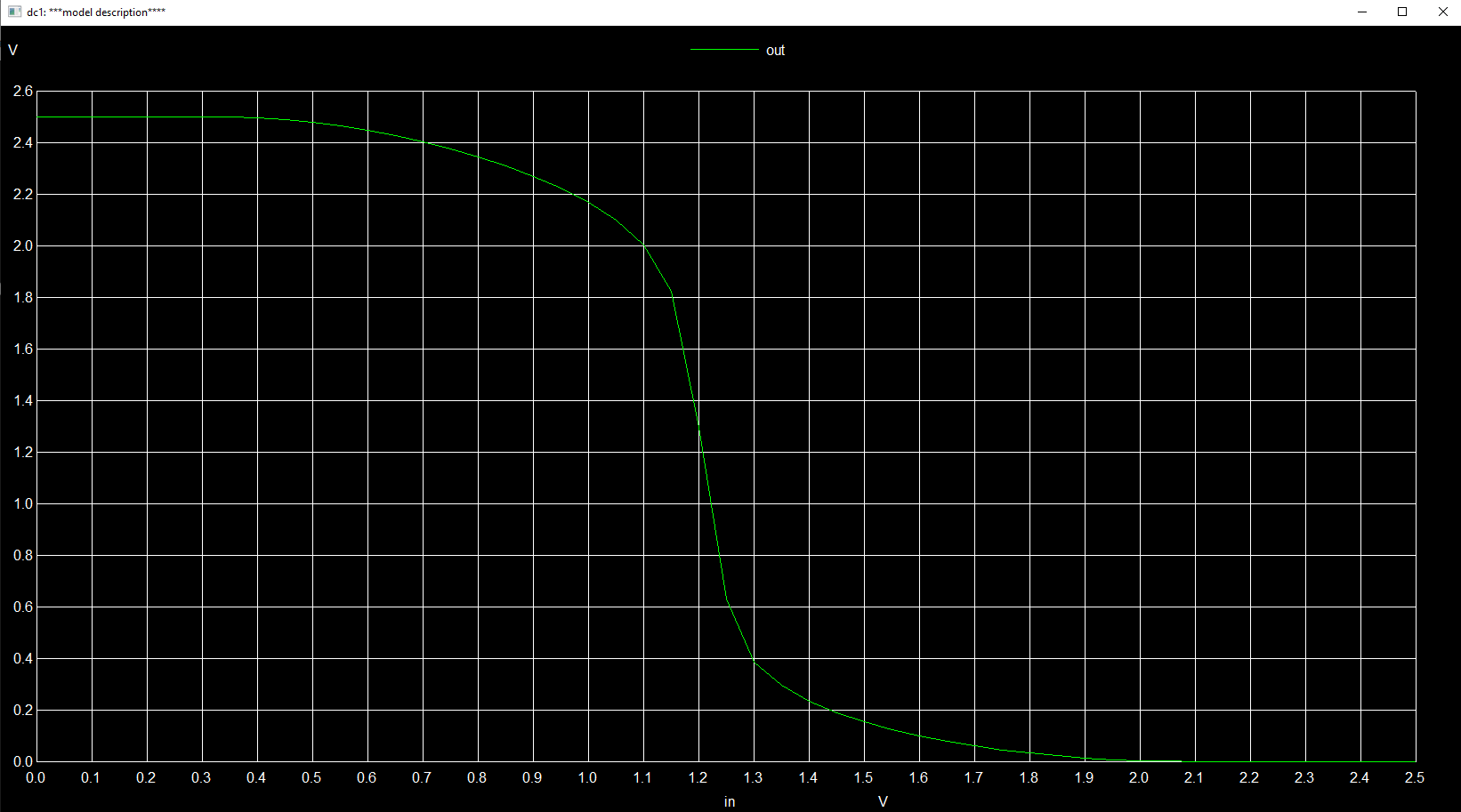
From the above we can see that the switching threshold of the latter is exactly midway with reference to Vdd and is slightly shifted to the left with the former
At the Switching threshold pmos and nmos drain add up to zero. Using this condition and the Drain Current equation we can fix a value for W/L to obtain the required switching voltage
From this the thresholds timings are characterised
Refer Nickson-Jose Git Repo for the files
The objective is to insert the custom designed inverter into the openlane flow
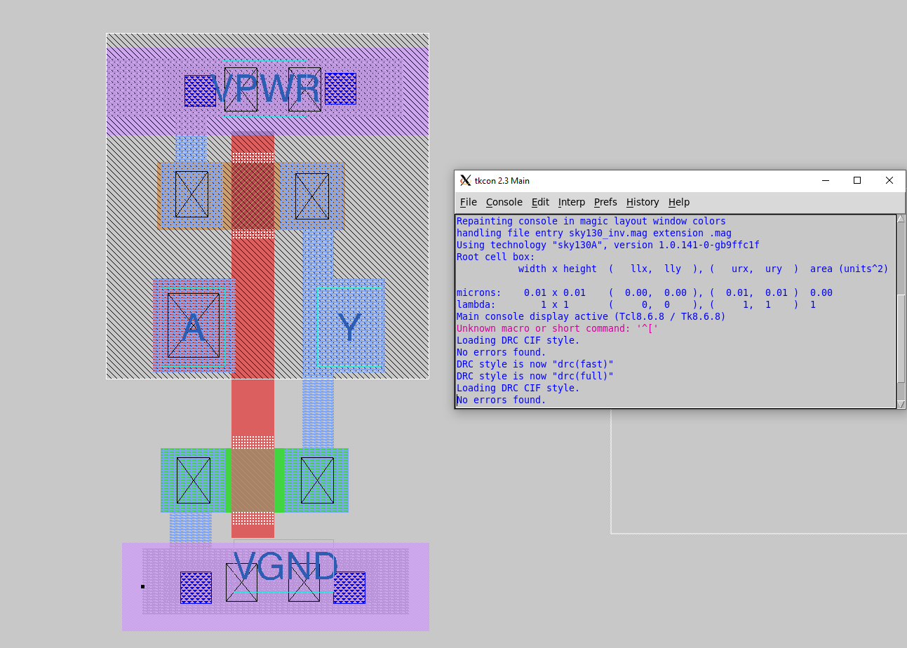
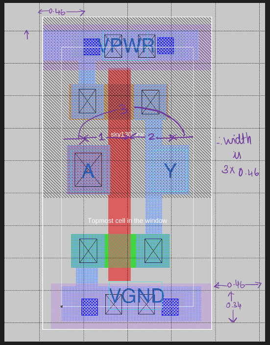
Open the sky130_inv.mag file in magic
-
DRC is checked. To place in the openLANE flow we need the LEF File only.
-
LEF is the Library Exchange Format.
-
It has only the information of the metal layers.
-
It has no information of the function.
-
Because only the metal contacts are sufficient enough to do the placement.
-
This allows for protection of the IP of the vendor so the buyer cant reverse engineer the design as a single LEF can enumerate to multiple Layouts as the number of possible interconnection keep increasing with intersections and the layers
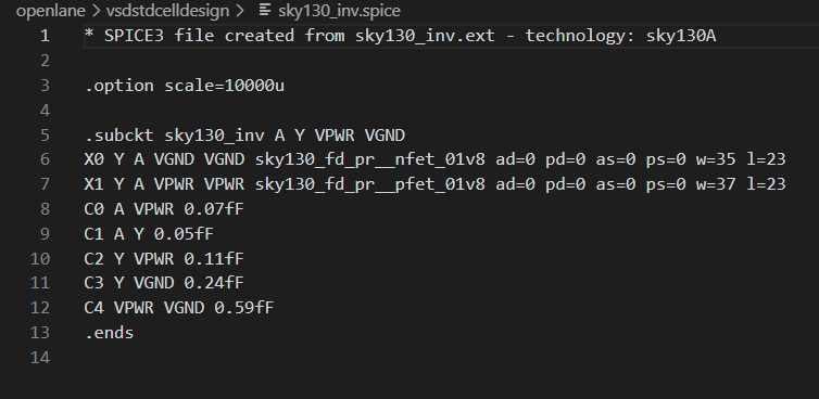
Extract the SPICE file
Extracted Spice File
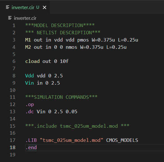
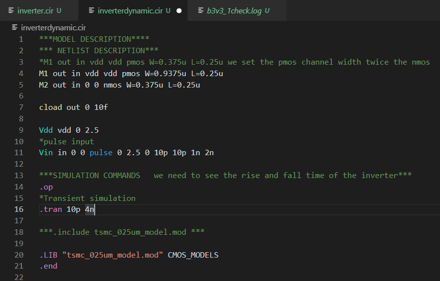
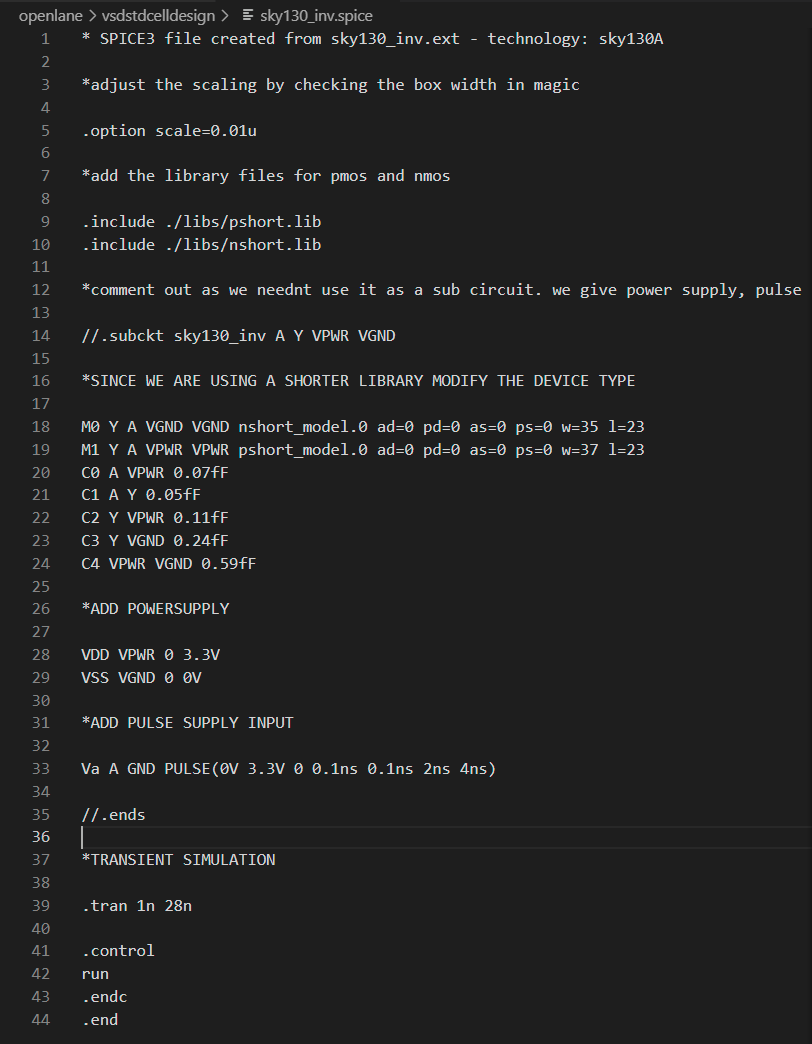
The following test circuit has to be implemented.
Edited SPICE Deck
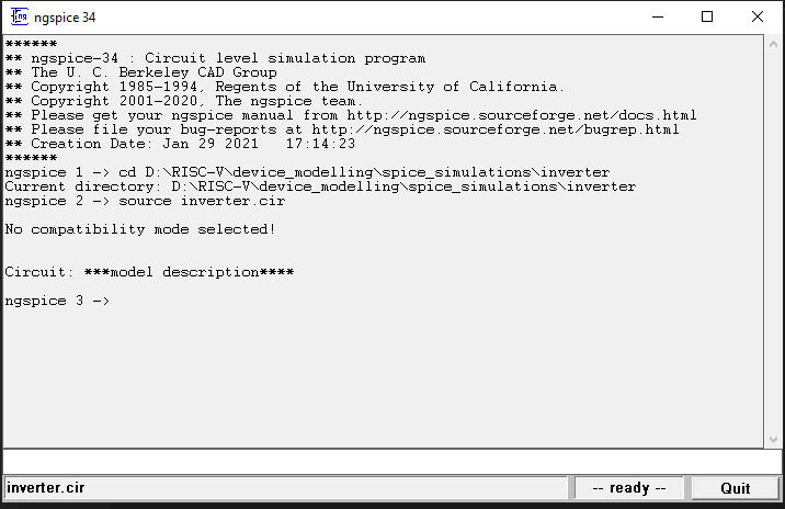
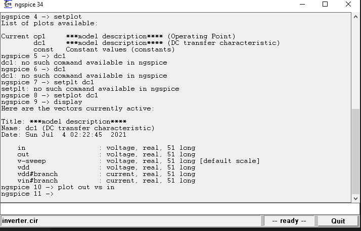
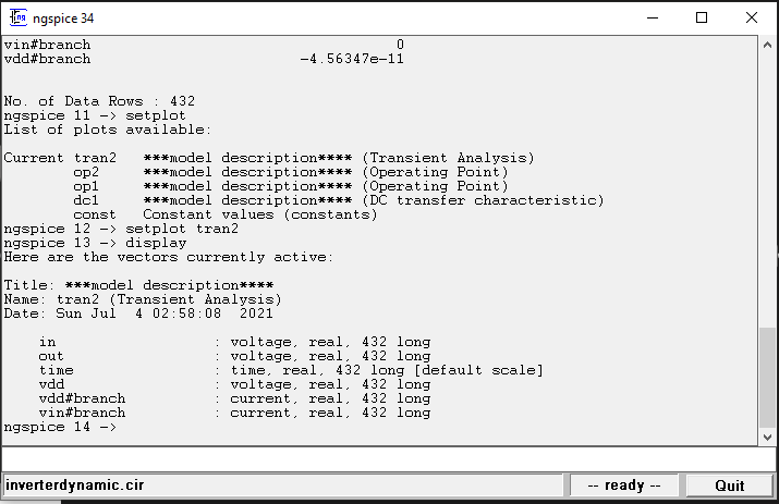
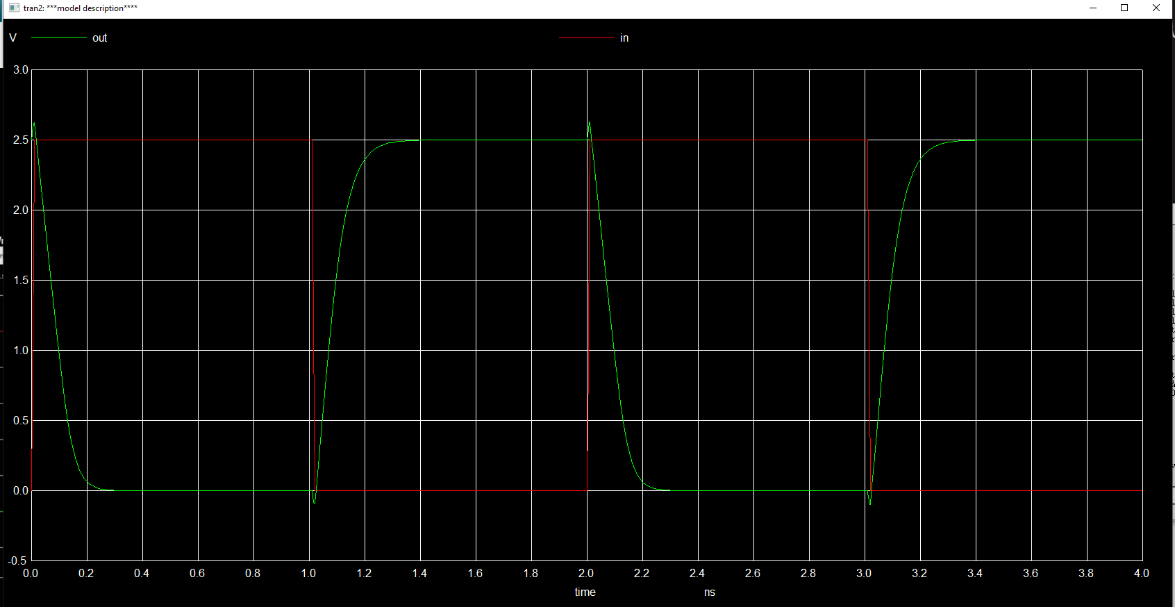
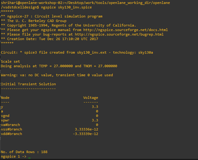
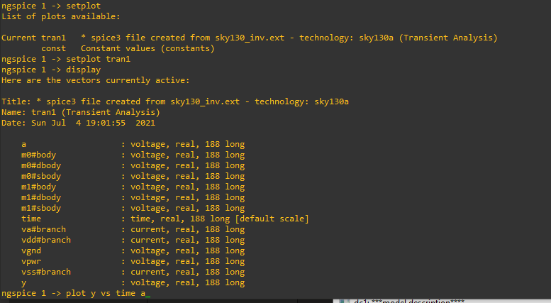
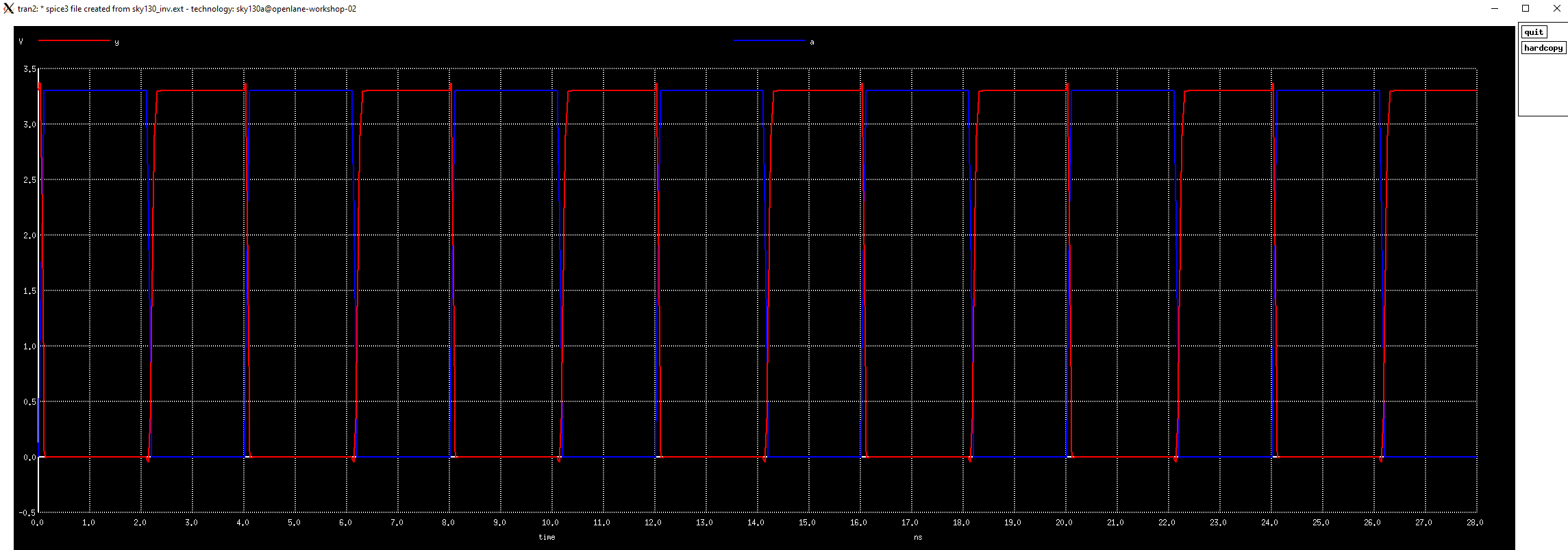
Ngspice simulation
From the graph manually timing characterisation is done
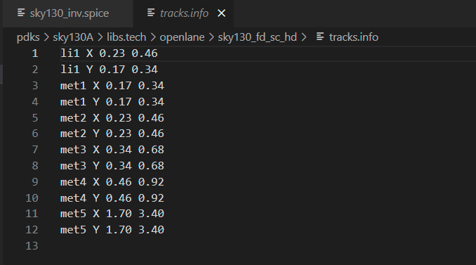
To make the standard cells to be used in the PnR the following rules are followed
- The input and output ports must lie on the vertical and horizontal tracks
- The width of the standard cell muse be odd multiple of the track pitch
- The height of the standard cell must be odd multiple of the vertical pitch
tracks.info file contains this information
Adjust grid accordingly so that the geometry can be interpreted with the track information
In the Layout file the ports are defined,as the LEF file requires only ihe information of the ports by using magic edit>text
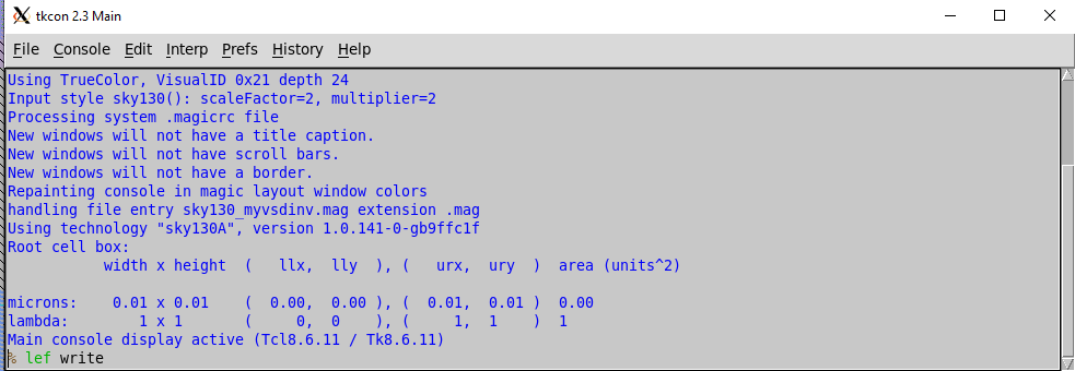
Extract the lef file
Extracted LEF File
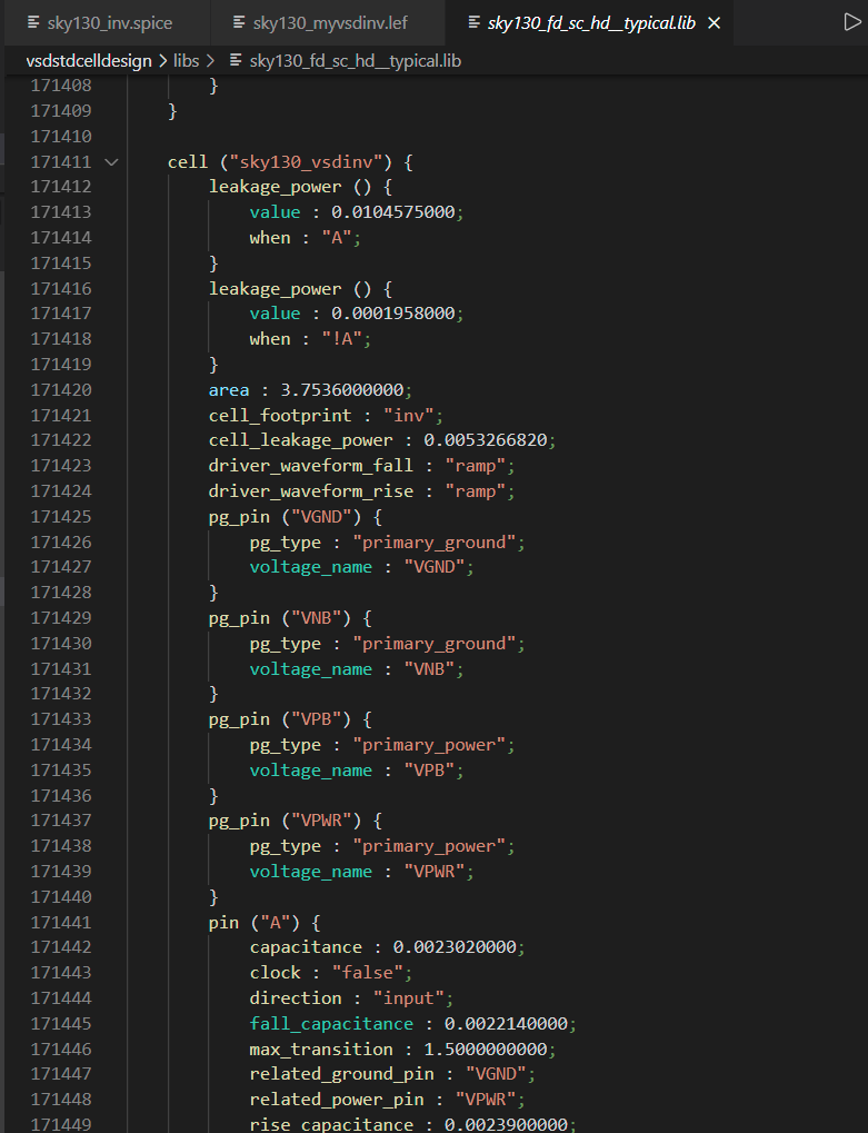
The standard cell is included in the skywater library
Copy the libraries and lef file the the design source folder
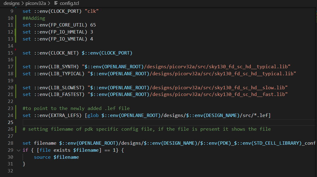
Edit the config.tcl in the design folder as shown below
In openlane enter the following to include the lef ile
Run Synthesis
It can be seen that the added cell is included
Go to the /openlane_ROOT/designs/runs/t1/reports/synthesis directory to see the OpenSTA timing reports
After synthesis the total negative slack and worst negative slack can be seen
Maximum Slack violation observed
Adjusting the syntesis parameters
SYNTH_STRATEGYis set asDELAY 1to optimise the timing and tradeoff the areaSYNTH_SIZINGto allow including various sizes of the standard cells to optimise the timing- Changes are made with the following commands in openlane.
set ::env(SYNTH_STRATEGY) "DELAY 1"
set ::env(SYNTH_SIZING) 1
- The commands can also be included in the cofig.tcl file but the run has to be overwritten
After modification the synthesis reported as follows
We can see that the area is increased and the number of cells are also increased
Maximum Slack
Minimum Slack
Now run_floorplan. This generates a picorv32a.floorplan.def
To avoid errors follow the below steps to perform the floorplan and placement
init_floorplanplace_ioglobal_placement_ordetailed_placementtap_decap_ordetailed_placement
Click here to view the logs, reports and results
DEF File after Placement
This CTS is performed on the placement .def file. Since that is the recently run
- In openlane type
openroad - Read the lef file
read_lef /openLANE_flow/designs/picorv32a/runs/t3/tmp/merged.lef
- Read the Def file
read_def /openLANE_flow/designs/picorv32a/runs/t3/results/cts/picorv32a.placement.def
- Create the db
write_db pico_cts_2.db
- Preform Analysis using OpenSTA inside openroad
read_db pico_cts_2.dbread_verilog /openLANE_flow/designs/picorv32a/runs/t3/results/synthesis/picorv32a.vread_liberty $::env(LIB_SYNTH_COMPLETE)link_design picorv32aread_sdc /openLANE_flow/vsdstdcelldesign/extras/my_base.sdc- Set the clock buffer to use from 2
set ::env(CTS_CLK_BUFFER_LIST) [lreplace $::env(CTS_CLK_BUFFER_LIST) 0 0]set_propagated_clock [all_clocks]report_checks -format full_clock_expanded -digits 4- Minimum Slack
- Maximum Slack
Run the CTS and do the Post STA Analysis with the same steps
Run the CTS using run_cts
A .def file after cts is created and an optimised .v netlist is created in the synthesis folder
Def file after CTS
gen_pdn- Generate the Power Distribution network- The power distrubution network has to take the
design_cts.defas the input def file. - This will create the grid and the straps for the Vdd and the ground. These are placed around the standard cells.
- The standard cells are designed such that it's height is multiples of the space between the Vdd and the ground rails. Here, the pitch is
2.72. Only if the above conditions are adhered it is possible to power the standard cells. - The power to the chip, enters through the
power pads. There is each for Vdd and Gnd - From the pads, the power enters the
rings, through thevia - The
strapsare connected to the ring. Vdd straps are connected to the Vdd ring and the Gnd Straps are connected to the Gnd ring. There are horizontal and the vertical straps - Now the power has to be supplied from the straps to the standard cells. The straps are connected to the
railsof the standard cells - If macros are present then the straps attach to the
ringsof the macros via themacro padsand the pdn for the macro is pre-done. - There are definitions for the straps and the railss. In this design straps are at metal layer 4 and 5 and the standard cell rails are at the metal layer 1. Vias connect accross the layers as required.
run_routing- To start the routing- The options for routing can be set in the
config.tclfile. - The optimisations in routing can also be done by specifying the routing strategy to use different version of
TritonRoute Engine. There is a trade0ff between the optimised route and the runtime for routing. - For the default setting picorv32a takes approximately 30 minutesaccording to the current version of TritonRoute.
- This routing stage must have the
CURRENT_DEFset topdn.def - The two stages of routing are performed by the following engines
- Global Route : Fast Route
- Detailed Route : Triton Route
- Fast Route generates the routing guides, whereas Triton Route uses the Global Route and then completes the routing with some strategies and optimisations for finding the best possible path connect the pins.
- The routing has been complted without any DRC violations.
- RC Extraction is done and the SPEF File is generated in the
picorv32a/runs/03-07_16-12/results/routing/picorv32a.spef - The routing guides produced in each stage of the routing is present in the
run/run_name/tmp/routingdirectory - In the current version of OpenLane (Openlane 0.21), the SPEF Extractor is built-in. So on running the routing the Parasitics are extracted and Post-routing STA is performed.
- In the older versions of openlane, the SPEF Extraction has to be done manually and the STA has to be performed in Openroad by creating a new db with the new
deffile and the appropriate verilog netlists.
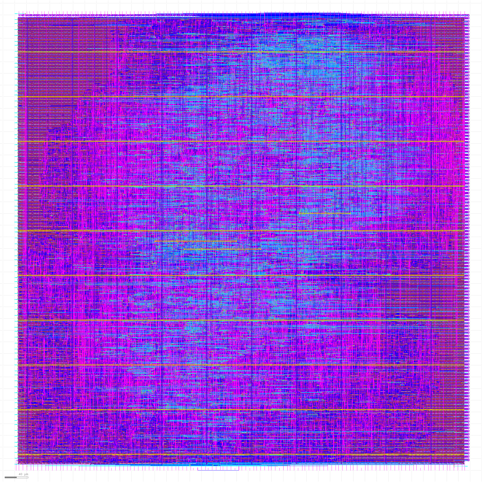
Final DEF File after routing
GDS Stands for Graphic Design Standard. This is the file that is sent to the foundry and is called "tape-out"
Fact- Earlier, the GDS files were written on magnetic tapes and sent out to the foundry and hence the name "tape-out"
In openLane use the command run_magic
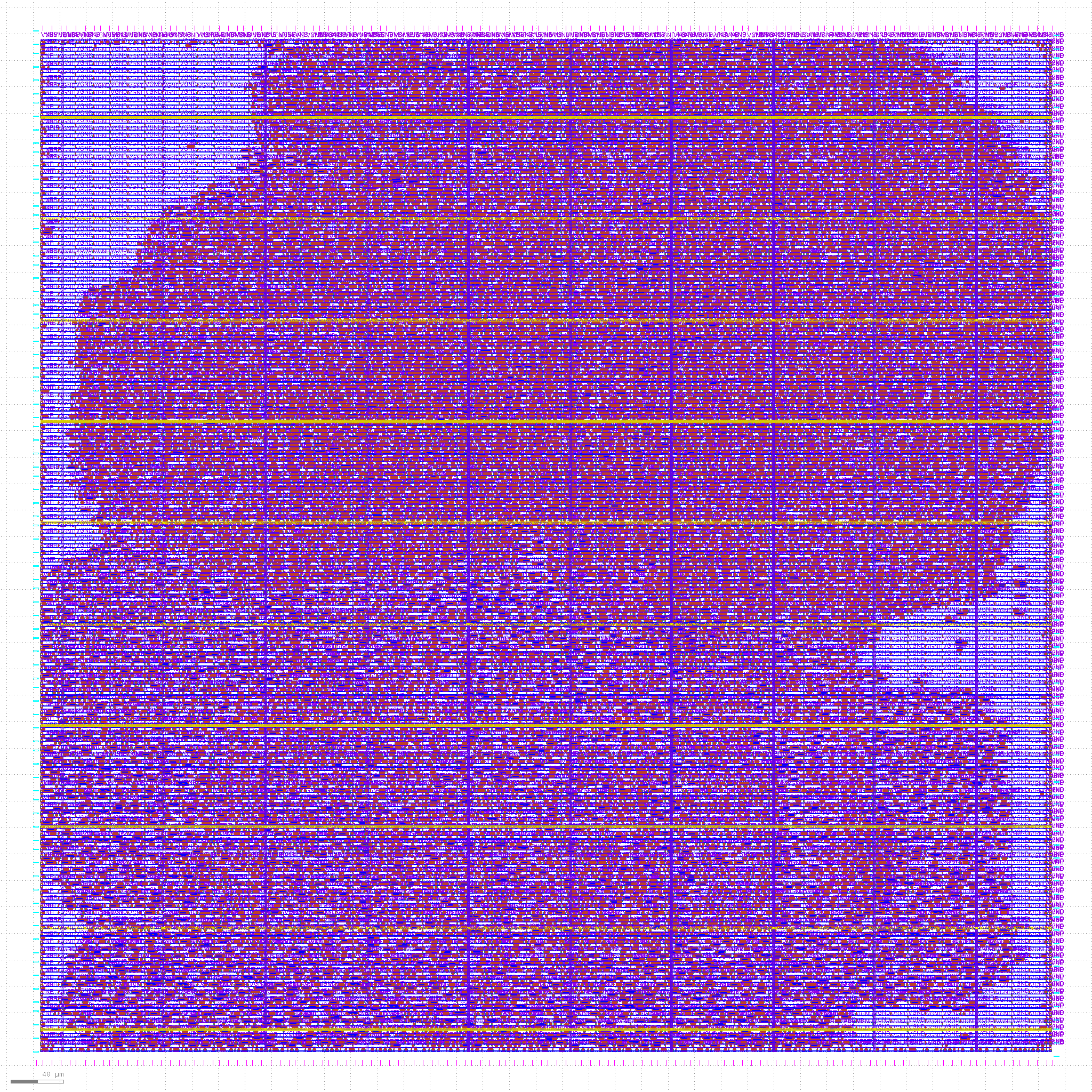
The GDSII file is generated in the results/magic directory
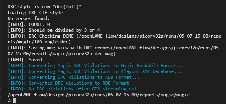
Checking DRC using run_magic_drc
No DRC errors are found.
Opening the GDSII file in klayout


