This project was performed on the completion of our four-week-long B. Tech 4th Semester Summer Training cum Academic Internship Programme on "RISC-V based 32-bit Digital Processor Design using SPICE" under Electronics & ICT Academy, IIT Guwahati and Assam Science & Technology University, Guwahati under TEQIP III in association with VLSI Expert Private Ltd during July-August, 2020.
- ASTU__180610026032 - schematics for basic digital gates, adders, mux, filters, multipliers, etc.
- Figures - all the figures used in the final report.
- Output Images - schematics/test-bench images and simulated signal outputs
- Project_Schematics - multiplier schematics used in the project
- TechnoReady_VLSIExpert_DigLib - schematics provided by VLSI Expert
- images - 16/32-bit multiplier schematics and simulation images
32 BIT MULTIPLIER_block_diagram.jpg32-bit Multiplier Design Presentation.pptx32-bit Multiplier design.docxFinal Report.pdf
- Abstract
- Introduction
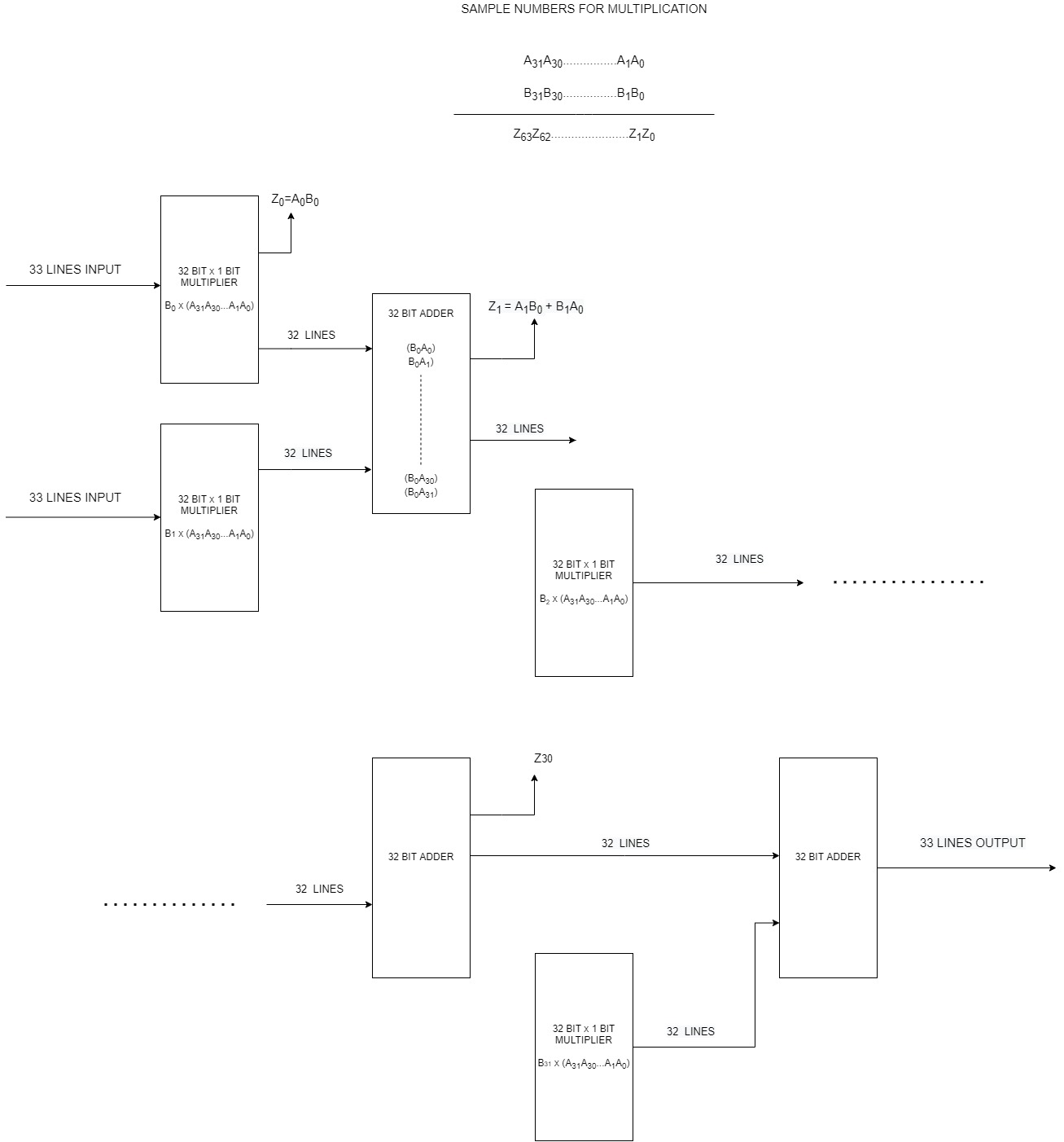
- Architecture
- Software Used
- Circuit Schematics
- Result Analysis
- Simulation Plots
This project involves designing and simulating a 32-bit multiplier using transistor-level digital gates in SPICE. The design is structured with AND operation of one 32-bit number with the first bit of a second 32-bit number to get the first bit of the 64-bit product and repeating the same process with the second bit of the second 32-bit number, then adding the result to get the second bit of the 64-bit product and further iterating these steps for the consecutive bits of the second 32-bit number and adding it to get the next bit of the 64-bit product. We successfully obtained the output for the logic in a 16-bit multiplier. However, due to the underperformance of the low-end device, the 32-bit model of the multiplier could not be tested. It implies, the logic carried out to tackle the problem was correct.
A multiplier follows the arithmetic operation where two numbers are multiplied. Multiplication is the fundamental operation in most digital signal processing(DSP) algorithms to perform functions like convolution, filtering and processing, so on. Recent statistics show that more than 69.90% of the instructions perform addition and multiplication in most of the microprocessor and DSP algorithms, i.e., these operations consume most of the execution time after simulation on compiling. In a system comprising of a multiplier, the system performance is usually determined by the performance of the multiplier as it is the slowest element of all. Hence, optimizing the speed of the multiplier is a crucial design issue. Due to the design complexity of different logic-circuit combinations in the implementation of 32-bit multipliers, execution gets slower or run-time increases. Therefore the prior multiplication process is divided into three steps: A. generating the partial products, B. reducing the partial products and C. addition to getting the final product. The speed of multiplication can be improved by reducing the generated number of partial products, thus increasing the speed at which these partial products are accumulated. The proposed solution of a 32-bit multiplier is to provide a compact utilization, high speed and low power consumption unit at a certain level of implementation for better speed and power usage.
The combinational logic components used are: 32-bit full adders, 32-bit AND gates, input and output lines to display the output in CPPsim and the general purpose of multiplication of bits.
-
Adder - Multiplication employs addition in its operations, and its hardware is similar if not identical to additional hardware. Thus, an adder or multiple adders will be in the critical path of the design; the performance of implementation will be often limited by the performance of its adders. When we look at other attributes of a chip, such as an area or power, we see that the hardware for addition will be a huge contributor to these areas. Hence it is beneficial to choose the correct adder to implement in a design. A Ripple Carry Adder is a logical circuit using multiple full adders (FA) to add N-bit numbers. Each FA inputs a carry Cin which is the Cout of the previous adder. This kind of adder is a Ripple Carry Adder (RCA) since each carry-bit "ripples" to the next full adder. The first FA can be replaced by a Half Adder(HA). The layout of an RCA is simple, which allows fast design time. However, the ripple carry adder is relatively slow as it has to wait for the carry bit that arrives from the previous full adder.
Sum (Si) = (Ai xor Bi) xor Ciandcarry (Ci+1) = (Ai and Bi) or (Ci and (Ai xor Bi)) -
AND gate - The output state of a digital logic AND gate only returns “LOW” again when any of its inputs are at a logic level “0”. In other words for a logic AND gate, any LOW input will give a LOW output.
The design consists of feeding the first 32-bit number with the first bit of the second 32-bit number to 32*1 AND gates and then extracting the first bit of the 64-bit output ( A0B0 ). We again do the same operation with B1, i.e., the second bit of the second 32-bit number and then add the two partial products with the help of a 32-bit Full Adder circuit to get the second bit of the 64-bit output, i.e., A1B1 + A0B1, and then iterate these steps for 31 times to get the left part of the 64-bit number. The rest bits are extracted from the last Full Adder (Number 31) output.
- 32-bit Multiplier
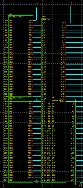
- Zoomed View
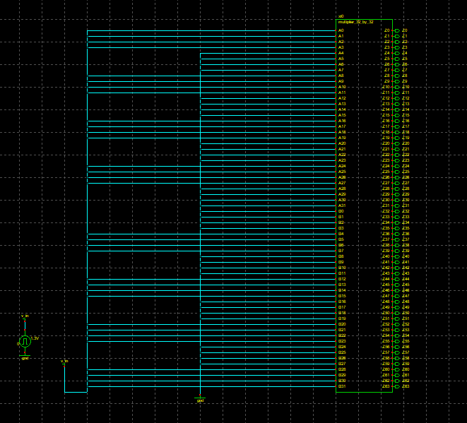
- Test-bench
We used the following two numbers for testing:
Input 1: 1111001111001111 ---- 62415 ( decimal form )
Input 2: 1010101010101010 ---- 43690 ( decimal form )
Output: 10100010100010010101110101110110 ( Theoretical ) ---- 2726911350 ( decimal form )
To supply the first 32-bit input we connected the input pins:
A0 A1 A2 A3 A6 A7 A8 A9 A12 A13 A14 A15 to the pulse signal (1)
and
A4 A5 A10 A11 to the ground (0)
For the second 32-bit input we connected the following input pins:
A1 A3 A5 A7 A9 A11 A13 A15 to the pulse signal (1)
and
A0 A2 A4 A6 A8 A10 A12 A14 to the ground (0)
v_in( input signal )
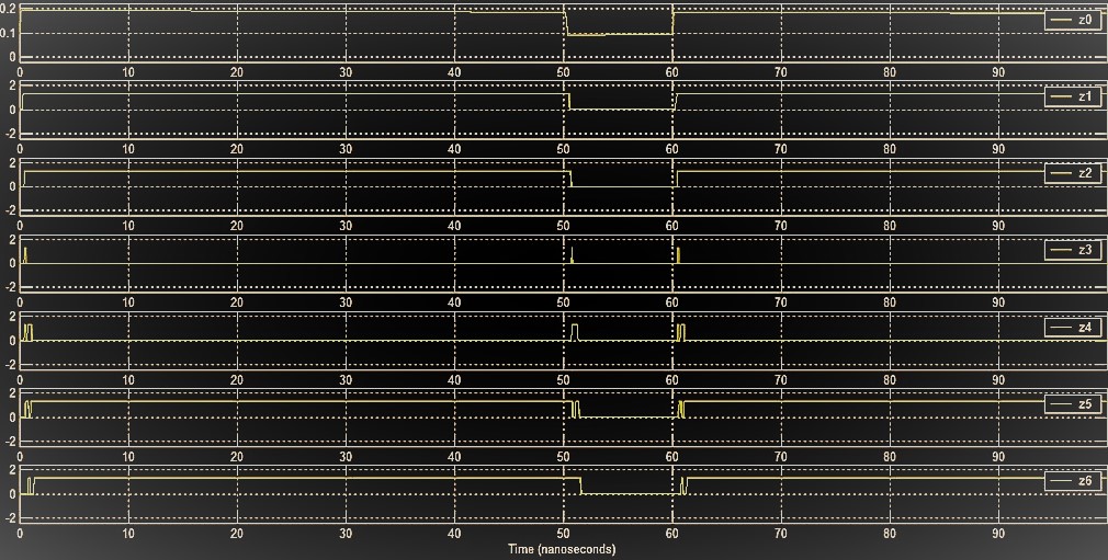
z0toz6
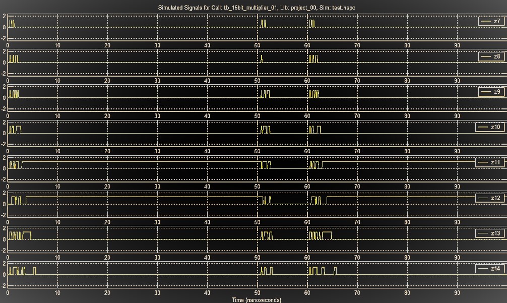
z7toz14
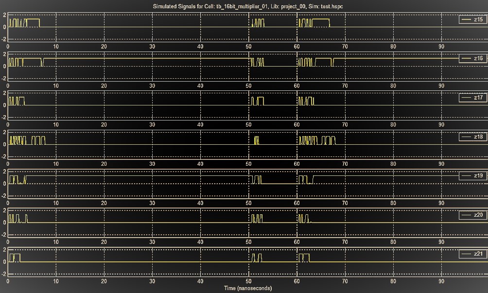
z15toz21
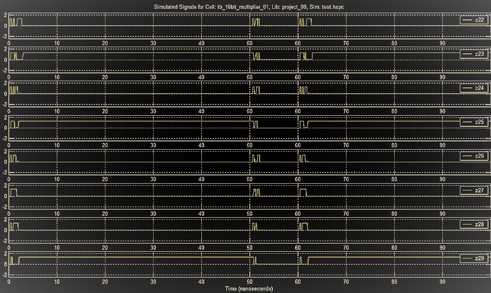
z22toz29
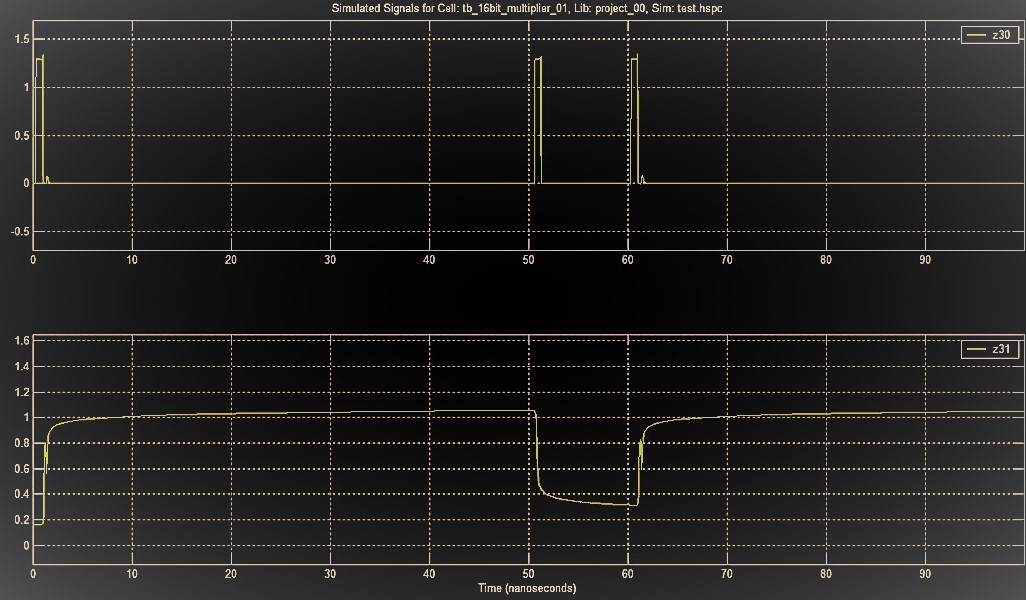
z30andz31

