-
To build KC705 bitstream file:
$ cd sv/prj/impl/kc705 $ make -
To build and run full system unisim RTL simulation:
$ cd sv/prj/impl/asic_sim $ make build $ make gui -
To build and run precise SystemC simulation (see github actions):
  $ cmake -S ./debugger/cmake -B build
  $ cd build
  $ make
  $ cd linuxbuild/bin
  $ ./run_sysc_river_x1_gui.sh
Note: Information related to VHDL source code is obsolete and currently is updating.
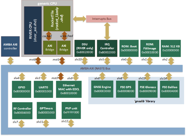
This repository provides open source System-on-Chip implementation based on open source RISC-V specifications. SOC project includes general set of peripheries, FPGA CADs projects files, own implementation of the Windows/Linux debugger and several examples that help to run your firmware on almost any FPGA boards. Satellite Navigation (GPS/GLONASS/Galileo) modules were stubbed in this repository and can be requested separately.
That's a VHDL RISC-V ISA implementation used in a several projects including
the multi-sytem Satellite Navigation receiver. It is great for an
embedded applications with active usage of 64-bits computations (like DSP).
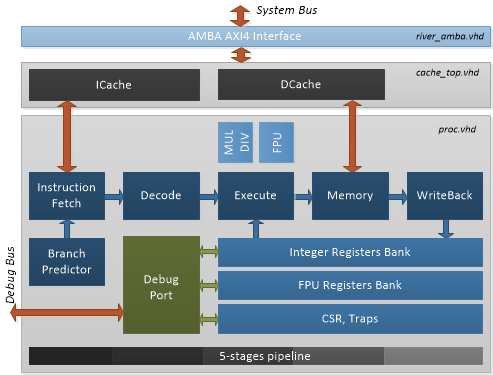
River CPU includes the following tools and features:
- Source code
- /debugger/cpu_fnc_plugin - Functional RISC-V CPU model.
- /debugger/cpu_sysc_plugin - Precise SystemC RIVER CPU model.
- /rtl/riverlib - synthesisable VHDL model of a 64-bit processor compliant with the RISC-V architecture.
- Floating Point Unit (FPU)
- Multi-Core configuration
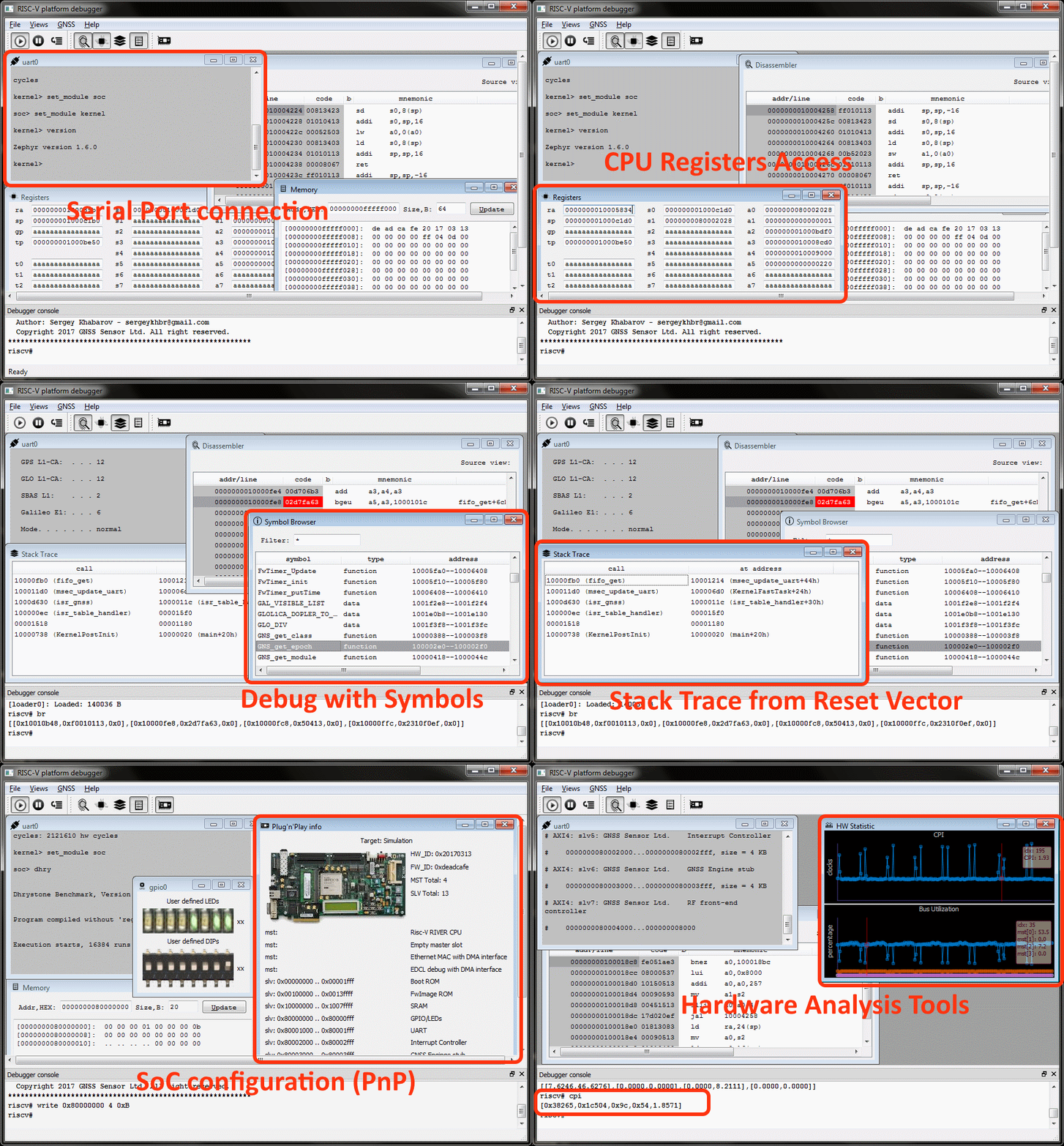
- Advanced debugging features
- Test Access Points (TAPs) via Ethernet, UART and JTAG in one system.
- Compatible with the Standard RISC-V debug specification.
- System Bus tracer
- Pipeline statistic (CPI, HW stacktrace) in a real-time on HW level.
- Plug'n'Play information
You can find several demonstration videos here of working with the Dual-Core SoC on FPGA and with the emulated platforms.
SoC documentation in .pdf formats.
Performance analysis is based on very compact Dhrystone v2.1. benchmark application available as the bare-metal test in $(TOP)/example/dhrystone21 folder and entirely ported into Zephyr shell (see animated gif below). Benchmark was executed with enabled (-O0) and disabled (-O2) optimization to define HW and GCC-compiler advantages. All sources are available and could be run on the simulator or on the different FPGA targets.
| Target | Git tag | Dhrystone per sec, -O0, 60 MHz |
Dhrystone per sec, -O2, 60 MHz |
Information. |
|---|---|---|---|---|
| RISC-V simulator | latest | 76824.0 | 176469.0 | GCC 7.1.1 with the compressed instructions set. |
| RISC-V simulator | latest | 77719.0 | 184074.0 | GCC 8.3.1 with the compressed instructions set. |
| "River" CPU | latest | 48581 | 135432.0 | GCC 8.3.1 with the compressed instructions set. |
| ARM simulator | latest | 78451.0 | 162600.0 | arm-none-eabi-gcc 7.2.0, ARM ISA only. |
| Cortex-R5 ARM | No | 20561.0 | 42401.0 | arm-none-eabi-gcc 7.2.0, custom FPGA system: Single-Core, MPU enabled, Caches disabled. |
| Cortex-R5 ARM | No | 54052.0 | 132446.0 | arm-none-eabi-gcc 7.2.0, custom FPGA system: Single-Core, MPU enabled, Caches enabled. |
| Cortex-M3 Thumb2 | arm_vhdl | soon | soon | arm-none-eabi-gcc 7.2.0, custom FPGA system |
| "LEON3" SPARC V8 | No | 48229.0 | 119515.0 | sparc-elf-gcc 4.4.2, custom FPGA system. |
Access to all memory banks and peripheries for all targets (including ARM and Leon3) is made in the same clock domain and always is one clock (without wait-states). So, this benchmark result (Dhrystone per seconds) shows performance of the CPU with integer instructions and degradation of the CPI relative ideal (simulation) case.
| CPU | Clocks-Per-Instruction, CPI |
Description. |
|---|---|---|
| Cortext-R5 | 1.22 | This is dual-issue processor capable to execute a pair of instructions per one clock. It's a very good but quite expensive CPU. |
| LEON3 | 1.5 | CPI information from here. |
| River | 1.35 | Free-to-use and highly customizable CPU. I/D caches are enabled: 4-ways, 16 KB each. Reference Manual. |
| Cortex-M3 | soon | RTL is under development. |
Since the tag 'v7.0' RIVER CPU is the main processor in the system and all issues related to Rocket-chip instance will be supported only by request.
This repository consists of three sub-projects each in own subfolder:
- rtl is the folder with VHDL/Verilog sources of the SOC
including synthesizable processors "Rocket" and "River" and peripheries.
Source code is portable on almost any FPGA is due to the fact that
technology dependant modules (like PLL, IO-buffers
etc) instantiated inside of "virtual" components
in a similar to Gailser's GRLIB way.
Full SOC design without FPU occupies less than 5 % of FPGA resources (Virtex6). "Rocket-chip" CPU itself is the modern 64-bits processor with L1-cache, branch-predictor, MMU and virtualization support.
This sub-project also contains:- fw_images: directory with the ROM images in HEX-format.
- prj: project files for different CADs (Xilinx ISE, ModelSim).
- tb: VHDL testbech of the full system and utilities.
- bit_files: Pre-built FPGA images for ML605 and KC705 boards.
- examples folder contains several C-examples that could help start working
with the RISC-V system:
- boot is the code of the Boot Loader. It is also used for the SRAM initialization with the FW image and it allows to run examples on FPGA without using the debugger and external flash memory.
- helloworld the simplest example with UART output.
- isrdemo example with 1 second interrupt from timer and debug output.
- zephyr is ported on RISC-V 64-bits operation system. Information about this Real-Time Operation System for Internet of Things Devices provided by Zephyr Project. Early support for the Zephyr Project includes Intel Corporation, NXP Semiconductors N.V., Synopsys, Inc. and UbiquiOS Technology Limited.
- debugger. The last piece of the ready-to-use open HW/SW system is Software Debugger (C++) with the full system simulator available as a plug-in. Debugger interacts with the target (FPGA or Software Simulator) via Ethernet using EDCL protocol over UDP. To provide this functionality SOC includes 10/100 Ethernet MAC with EDCL and Debug Support Unit (DSU) devices on AMBA AXI4 bus.
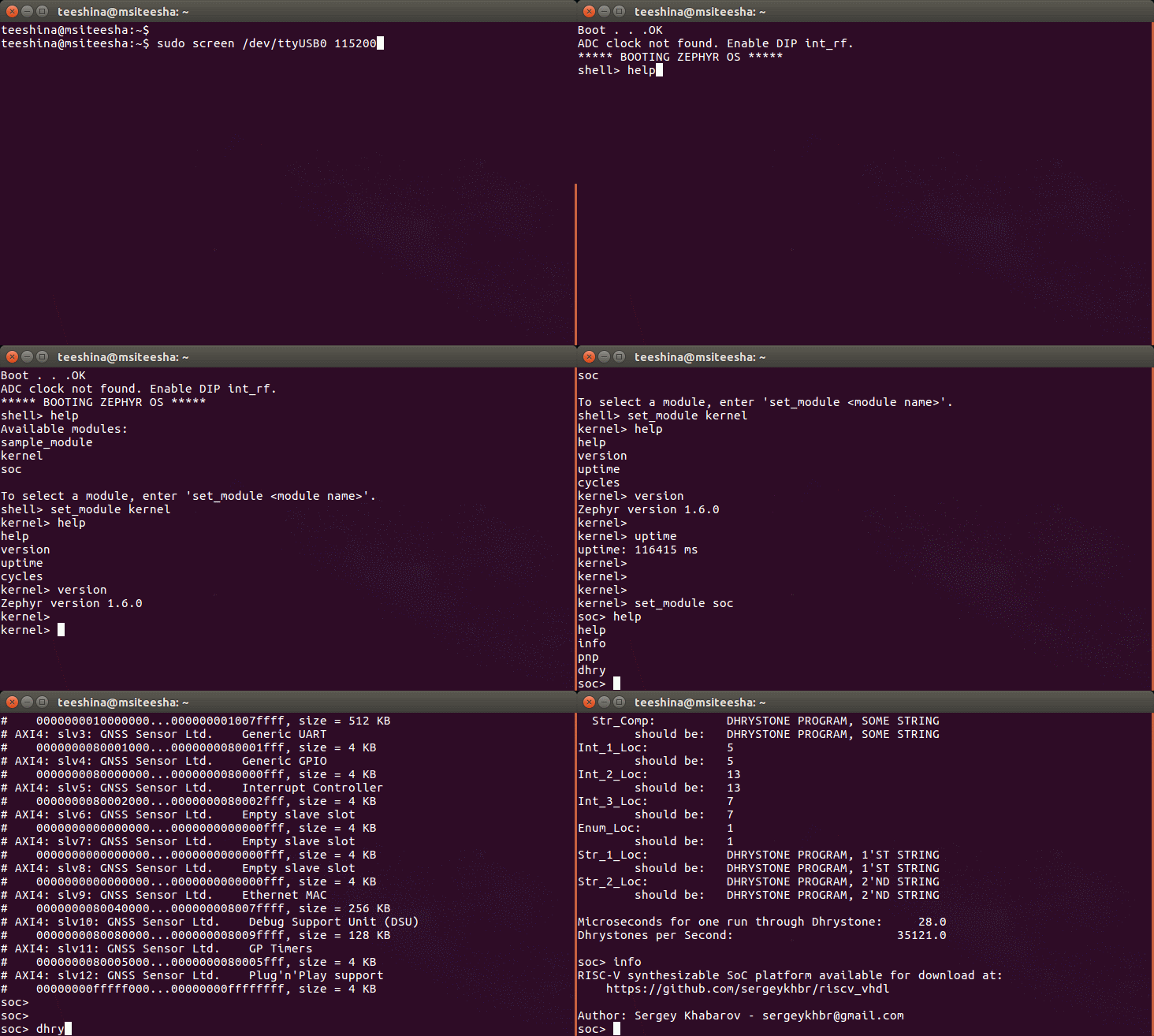
You can use the pre-built FPGA image (for Xilinx ML605 or KC705 board) and any serial console application (putty, screen or other) to run Dhrystone v2.1 benchmark as on the animated picture below.
-
Unpack and load file image riscv_soc.bit from /rtl/bit_files/ into FPGA board.
-
Connect to serial port. I used standard console utility screen on Ubuntu.
$ sudo apt-get install screen $ sudo screen /dev/ttyUSB0 115200 -
Use button "Center" to reset FPGA system and reprint initial messages (or just press Enter):
To end the session, use Ctrl-A, Shift-K
How to build simulator from scratch see here
It should look like the following:
There's dependency of two others open source projects:
Default VHDL configuration enables River CPU with full debug support.
- Open ML605 project file for Xilinx ISE14.7 prj/ml605/riscv_soc.xise or KC705 project file for Xilinx Vivado prj/kc705/riscv_soc.xpr.
- Edit configuration constants in file work/config_common.vhd if needed. (Skip this step by default).
- Use rtl/work/tb/riscv_soc_tb.vhd" testbench file to verify full system including CPU, UART, Timers, Ethernet, GPIO etc.
- Generate bit-file and load it into FPGA.


