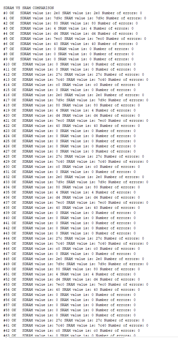
This project involves the integration and implementation of an SDRAM (Synchronous Dynamic Random-Access Memory) controller in Verilog. The SDRAM controller is designed to manage read and write operations to SDRAM memory using a finite state machine (FSM) to handle timing and command sequences. This README file provides an overview of the SDRAM controller, SDRAM model, and testbench for verification.
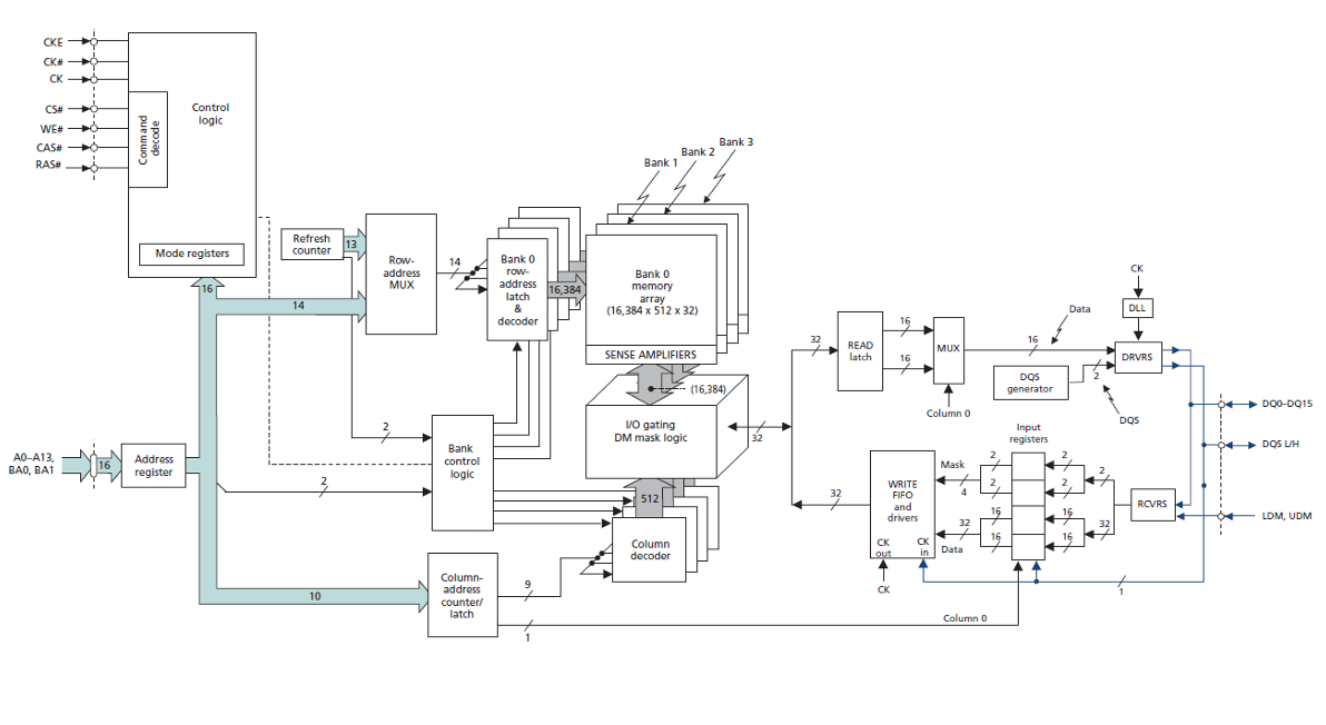
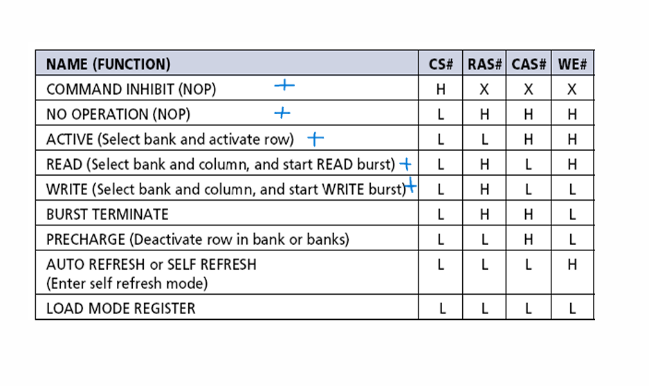
The SDRAM controller manages the timing and control signals required to interface with SDRAM memory. Supported commands are shown in blue. It supports the following operations:
- COMMAND INHIBIT (NOP): Invalid command.
- NOP (No Operation): Idle state for timing management.
- ACT (Activate): Activates a row in the SDRAM.
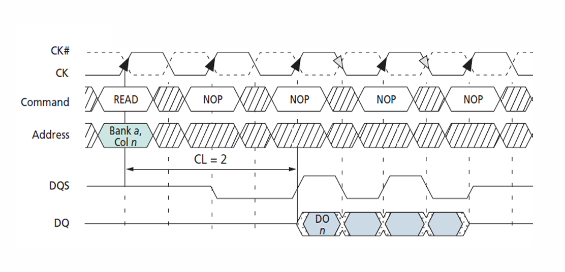
- READ: Reads data from the activated row.
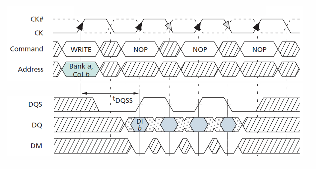
- WRITE: Writes data to the activated row.
- BURST TERMINATE: Ends the current burst operation. (Unsupported)
- PRECHARGE: Deactivates the open row in a bank. (Unsupported)
- AUTO REFRESH: Refreshes SDRAM contents to prevent data loss. (Unsupported)
- LOAD MODE REGISTER: Loads settings into the SDRAM mode register. (Unsupported)
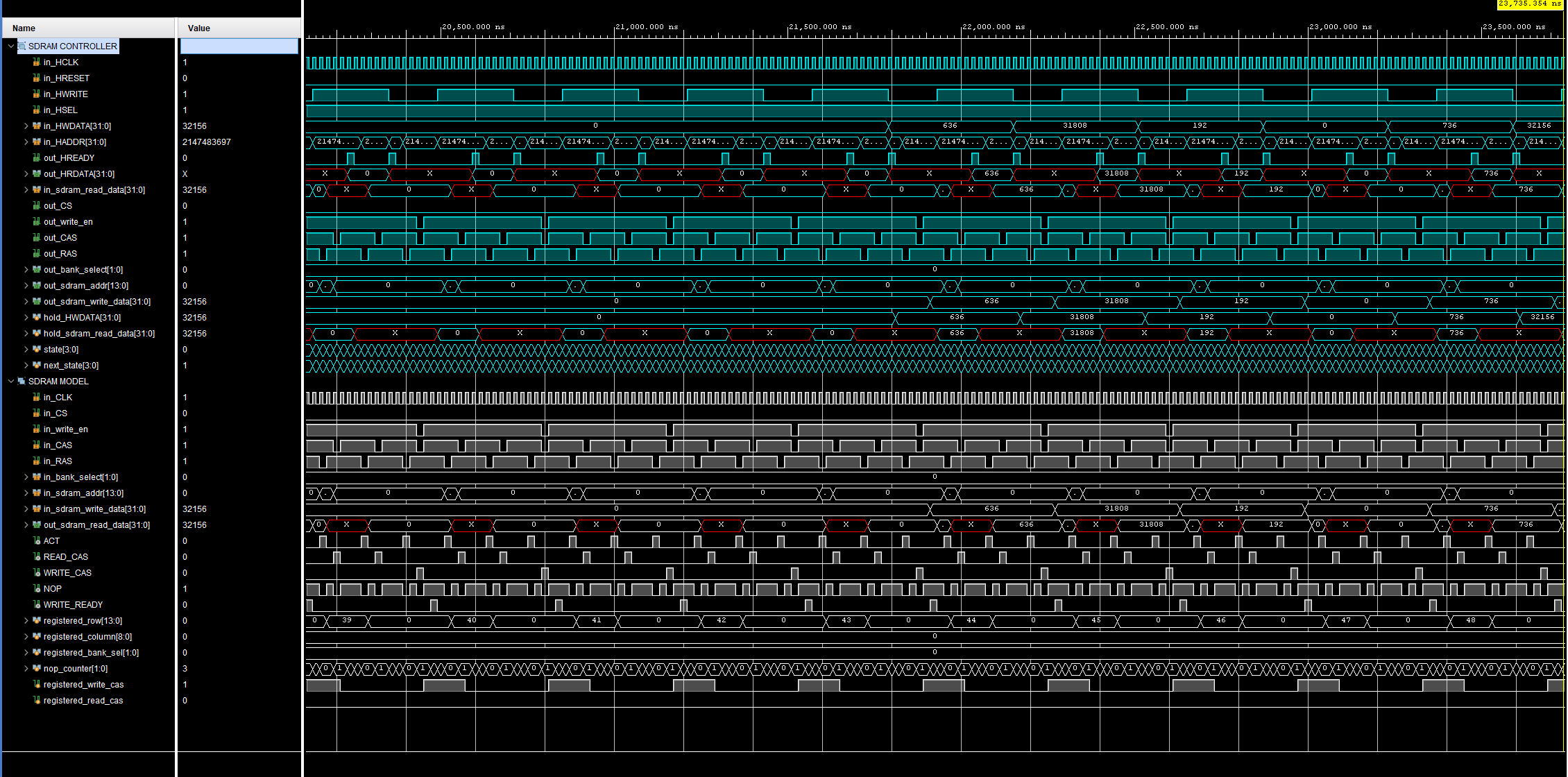
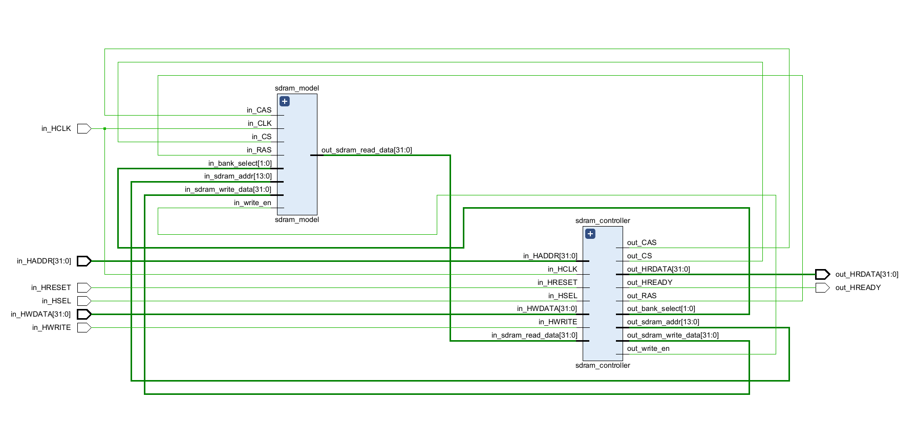
The SDRAM controller (sdram_controller.v) handles read and write operations using a finite state machine (FSM). The controller generates the necessary control signals (out_CS, out_write_en, out_CAS, out_RAS) and manages the address and data buses.
- Clock (
in_HCLK): System clock. - Reset (
in_HRESET): System reset. - Write Enable (
in_HWRITE): Indicates a write operation. - Slave Select (
in_HSEL): Selects the SDRAM controller as the active slave. - Address (
in_HADDR): Address bus. - Write Data (
in_HWDATA): Data bus for write operations. - Read Data (
out_HRDATA): Data bus for read operations.
- IDLE: Waits for a read or write request.
- READ_ACT: Activates a row for reading.
- READ_CAS: Sends column address for read.
- WRITE_ACT: Activates a row for writing.
- WRITE_CAS: Sends column address for write.
- NOP: Idle state for timing management.
- ACT (Activate): Activates a row in the SDRAM by providing the row address and bank select signals (
out_sdram_addr,out_bank_select). Prepares the SDRAM for read or write operations. - READ: Reads data from the activated row. Involves sending column address and bank select signals (
out_sdram_addr,out_bank_select) after the ACT command. - WRITE: Writes data to the activated row. Involves sending column address and bank select signals (
out_sdram_addr,out_bank_select) after the ACT command, followed by providing data (out_sdram_write_data) to be written. - NOP (No Operation): Idle states between commands where no action is taken. Allows for proper timing and sequencing of SDRAM operations. The NOP between ACT and CAS is necessary due to the RAS-CAS latency being 2 cycles, meaning there's a delay of 2 clock cycles between activating a row (ACT) and accessing the column (CAS). This ensures that the SDRAM controller operates within the timing constraints of the SDRAM protocol.
The SDRAM model (sdram_model.v) simulates the behavior of an actual SDRAM chip. It handles the read and write operations based on the control signals from the SDRAM controller.
- Chip Select (
in_CS): Selects the SDRAM chip. - Write Enable (
in_write_en): Enables write operations. - Column Address Strobe (
in_CAS): Activates column address. - Row Address Strobe (
in_RAS): Activates row address. - Bank Select (
in_bank_select): Selects the memory bank. - SDRAM Address (
in_sdram_addr): Address bus for SDRAM. - SDRAM Write Data (
in_sdram_write_data): Data bus for write operations. - SDRAM Read Data (
out_sdram_read_data): Data bus for read operations.
- Parameter Definitions: Data width (
DATA), row count (ROW), and column count (COLUMN). - Internal Signals: Signals such as
ACT,READ_CAS,WRITE_CAS,NOP, andWRITE_READYare defined based on the input signals to manage SDRAM operations. - Registers: Registers hold row, column, bank select, and NOP counter values during operations.
- Clocking Block: Updates the registers based on input signals and manages the NOP counter.
- Combinational Block: Handles SDRAM read and write operations based on the state of
WRITE_READYandin_write_ensignals. Uses a case statement to select the appropriate bank for read or write operations.
The project is organized as follows:
/docs       Project documentation
/src        Source files for SDRAM controller and model
/testbench  Testbench files for verification
- Write testbench: Create a comprehensive testbench file for the design.
- Validate FSM with assertions: Use verification methods like assertions to ensure FSM correctness.
